In the semiconductor design industry, most of the designs are created and optimized at the RTL level, mainly through home grown scripts or manual methods. As there can be several iterations in optimizing the hierarchy for physical implementation, it’s too late to do the hierarchical optimizations after reaching the floor plan… Read More

Tag: verilog
Crossfire – Your partner for IP development, what’s new?
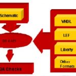
As the SoCs and IPs grow in sizes and complexities, the number of formats, databases, libraries of standard cells and IOs also increase. It becomes a clumsy task to check every cell in a library, its consistency among various format with respect to functionality, timing, naming, labels and so on, and its complex physical properties… Read More
Open Source Verilog
Over the years there have been various open source EDA projects but none that has realized a full industrial strength design tool that has broad adoption and is strong enough to compete with similar products from the EDA industry.
Open source is clearly a great way to develop software. Lots of people can see all the source code and … Read More
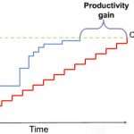
Enabling Higher Level Design Automation with Smart Tools
Although design houses have always strived for optimizing best design flows according to their design needs by customizing the flows using effective and efficient internal as well as external tools, this need has further grown in the context of design scenarios getting wider and wider from transistor, gate and RTL to system level.… Read More
Then, Python walked in for verification

Go ahead – type “open source” into the SemiWiki search box. Lots of recent articles on the IoT, not so many on EDA tools. Change takes a while. It has only been about five years since the Big Three plus Aldec sat down at the same table to work on UVM. Since then, Aldec has also gotten behind OS-VVM, and is now linked to a relatively new open… Read More
A Brief History of Functional Verification
Usually these brief history pieces are totally written by the SemiWiki blogger whose name is at the top. Often me since that was how I prototyped book chapters (buy). Well, OK, I did actually write this but it is completely cribbed from a presentation earlier this week by Wally Rhines who gave a sort of keynote at the announcement of… Read More
Mark your Date for Semiconductor Design Vision
A very popular acronym is ‘WYSIWYG’ – What You See Is What You Get! This is very true and is important to visualize things to make it better in various aspects such as aesthetics, compactness, organization, structure, understandable for correction and so on; the most important, in case of semiconductor design, is being able to identify… Read More
SoC Verification Closure Pushes New Paradigms
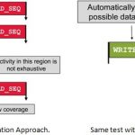
In the current decade of SoCs, semiconductor design size and complexity has grown by unprecedented scale in terms of gate density, number of IPs, memory blocks, analog and digital content and so on; and yet expected to increase further by many folds. Given that level of design, it’s imperative that SoC verification challenge has… Read More
Debugging Verification Constraints
In his DAC keynote last year (2012) Mike Mueller of ARM compared how much CPU was required to verify the first ARM versus one of the latest ARM Cortex CPUs. Of course the newer CPU is hundreds of times larger than the first ARM but the amount of verification required was millions of times as much, requiring ARM to construct their own datacenter… Read More
Accelera Technical Excellence Award

The Accellera Systems Initiative, most well-known for driving the standardization of various aspects of Verilog and SystemVerilog before handing the standards off to the IEEE, has announced that nominations are open for the 2013 Technical Excellence Award. This recognizes outstanding contributions in the creation of EDA… Read More