There have been a multitude of announcements recently relative to the incorporation of machine learning (ML) methods into EDA tool algorithms, mostly in the physical implementation flows. For example, deterministic ML-based decision algorithms applied to cell placement and signal interconnect routing promise to expedite… Read More
Tag: tsmc
Application-Specific Lithography: The 5nm 6-Track Cell
An update is now available here: Application-Specific Lithography: Patterning 5nm 5.5-Track Metal by DUV
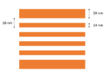
The 5nm foundry (e.g., TSMC) node may see the introduction of 6-track cells (two double-width rails plus four minimum-width dense lines) with a minimum metal pitch in the neighborhood of 30 nm. IMEC had studied a representative… Read More
Optimizing Chiplet-to-Chiplet Communications
Summary
The growing significance of ultra-short reach (USR) interfaces on 2.5D packaging technology has led to a variety of electrical definitions and circuit implementations. TSMC recently presented the approach adopted by their IP development team, for a parallel-bus, clock-forwarded USR interface to optimize power/performance/area… Read More
Multi-Vt Device Offerings for Advanced Process Nodes
Summary
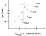
As a result of extensive focus on the development of workfunction metal (WFM) deposition, lithography, and removal, both FinFET and gate-all-around (GAA) devices will offer a wide range of Vt levels for advanced process nodes below 7nm.
Introduction
Cell library and IP designers rely on the availability of nFET and pFET… Read More
TSMC Pushes out Equip Purchases – SIA and SEMI ask for Government Help
TSMC pushing out equipment purchases
Covid/China trickles down to chip industry
SIA and SEMI ask for financial/govt help to keep up
The beginning of another down cycle?
We have heard from a number of sources that TSMC has started to push out equipment orders as concerns grow about the second half of the year.
Right now is the most logical… Read More
Time for Chip Diplomacy
An industry caught in the crosshairs of geopolitics needs global emeritus leadership
The semiconductor industry is at the epicenter of great power politics. An ascendant China is on a quest for a unified global system with China as the leading power. The United States seeks to maintain its position as leader of the liberal democratic… Read More
Effect of Design on Transistor Density
I have written a lot of articles looking at leading edge processes and comparing the process density. One comment I often get are that the process density numbers I present do not correlate with the actual transistor density on released products. A lot of people want to draw conclusions an Intel’s processes versus TSMC’s processes… Read More
China’s Position in the Global Semiconductor Value Chain
In this third article about China’s role in the global semiconductor industry I analyse the current state of affairs of the Chinese semiconductor industry in different segments. In the previous articles, I looked at the possible effects of a US-China decoupling in the semiconductor industry and the impact of the Big … Read More
eFPGA – What’s Available Now, What’s Coming and What’s Possible!
eFPGA is now widely available, has been used in dozens of chips, is being designed into dozens more and it has an increasing list of benefits for a range of applications. Embedded FPGA, or eFPGA, enables your SoC to have flexibility in critical areas where algorithm, protocol or market needs are changing. FPGAs can also accelerate… Read More
Cost Analysis of the Proposed TSMC US Fab
On May 15th TSMC “announced its intention to build and operate an advanced semiconductor fab in the United States with the mutual understanding and commitment to support from the U.S. federal government and the State of Arizona.”
The fab will run TSMC’s 5nm technology and have a capacity of 20,000 wafers per month (wpm). Construction… Read More


