You are currently viewing SemiWiki as a guest which gives you limited access to the site. To view blog comments and experience other SemiWiki features you must be a registered member. Registration is fast, simple, and absolutely free so please,
join our community today!
In a complex world of SoCs with multi-million gates and IPs from several heterogeneous sources, verification of a complete semiconductor design has become extremely difficult, and it’s not enough. In order to ascertain the right intent of the design throughout the design cycle, debugging at various stages of the design cycle… Read More
Usually these brief history pieces are totally written by the SemiWiki blogger whose name is at the top. Often me since that was how I prototyped book chapters (buy). Well, OK, I did actually write this but it is completely cribbed from a presentation earlier this week by Wally Rhines who gave a sort of keynote at the announcement of… Read More
In the 1990’s there was a push to build EDA frameworks, however they all failed because no user wanted to be locked into one EDA vendor tool flow. Fast forward to 2014 and there’s an emerging trend to use web-based EDA tools as a framework, instead of downloading and installing software to your desktop or device. I just… Read More
Mentor Graphics acquired Berkeley Design Automation this morning. The details of the deal were unannounced. This is a strong move by Mentor to challenge Cadence and Synopsys in the nanometer analog/mixed-signal market and nanometer memory characterization market, respectively. Mentor not only acquires the technology and… Read More
In this age of SoCs with hundreds of IPs from different sources integrated together and working at high operating frequencies, FPGA designers are hard pressed keeping up the chip reliability from issues arising out of excessive static & dynamic IR drop, power & ground noise, electro migration and so on. While the IPs are… Read More
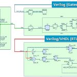
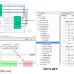
A very popular acronym is ‘WYSIWYG’ – What You See Is What You Get! This is very true and is important to visualize things to make it better in various aspects such as aesthetics, compactness, organization, structure, understandable for correction and so on; the most important, in case of semiconductor design, is being able to identify… Read More
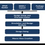
A semiconductor SoC design can have multiple components at different levels of abstractions from different sources and in different languages. While designing an SoC, IPs at different levels have to be integrated without losing the overall design goals. Of course, quality of an IP inside and outside of an SoC must be tested thoroughly.… Read More
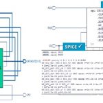
I’ve run SPICE circuit simulators since the 1970’s and they use transistor models where the device parameters are provided by the foundry. These transistor and interconnect parameters come from an engineer at the foundry who has characterized silicon with actual measurements or by running a TCAD (Technology CAD)… Read More
When we talk about parasitic, we talk about post layout design further expanded in terms of electrical components such as resistances and capacitances. In the semiconductor design environment where multiple parts of a design from different sources are assembled together into highly complex, high density SoC, imagine how complex… Read More
In an environment of SoCs with tough targets of multiple functionalities, smallest size, lowest power and fastest performance to achieve within a limited design cycle window in order to meet the rigid time-to-market requirements, any day spent without success becomes very frustrating for a designer. Especially during tape-out… Read More