If expanding industries typically indicate vibrancy, a race to acquire and consolidate is generally reflective of the opposite – a period of slowed growth in mature, once high-flying categories. And while many industries experience a period of stardom, followed by a sharp and steady decline, we should be extremely worried when… Read More
Tag: semiconductor design
Improve SoC Front-end Design Productivity
I have been involved in SoC developments for a long time. During this period I tried to learn what impacts the productivity and subsequently the market opportunity. Over the last year or so at SoCScape I have been involved designing solutions that can improve them. I have decided to post some of my thoughts here in a series of blogs … Read More
Four Industries that will be Transformed by GaN
In a previous post we discussed a few automotive applications that will be big markets for GaN technology. But this is just a small part of the GaN story!
GaN transistors such as eGaN FETs from EPC are today available with performance 10 times better than the best commercial silicon. What happens when several devices are integrated… Read More
The Intel Apple Deal is a Nothingburger!
The latest Intel rumor that the pro Intel media are flogging is that Intel modems will be in some of the new iPhones. The deal is estimated at around $1B. An “estimated” value of a “rumor” deal is quite funny in itself but let’s take a deeper look at what we are gossiping about here.
Intel got into the 3G/LTE business after acquiring the… Read More
CEVA in More than 6 Billion Chips!
One of the IP companies that I track is CEVA, the largest licensor of DSP cores. CEVA is the fifth largest IP company behind ARM, Synopsys, Imagination Technologies, and Cadence (Lattice acquired Silicon Image). CEVA is actually a combination of companies which started with the DSP Group and Parthus Technologies in 2002 and RiveriasWaves… Read More
Starvision and SOS, a Perfect Match
SoC design these days is largely about assembling externally developed semiconductor IP with a small amount of differentiated content. Only companies who have to adopt new processes instantly develop a lot of their own IP. It makes more sense to license it. Partially because there is not a lot of differentiation in standards-based… Read More
Conquering the Next IoT Challenges with FPGA-Based Prototyping
The need for ever-connected devices is skyrocketing. As I fiddle with my myriad of electronic devices that seem to power my life, I usually end up wishing that all of them could be interconnected and controlled through the Internet. The truth is, only a handful of my devices are able to fulfill that wish, but the need is there and developers… Read More
Which High B/W Memory to Select after DDR4?
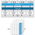
Once upon a time, RAM technology was the driver of the semiconductor process. DRAM products were the first to be designed on a newest technology node and DRAM was used as a process driver. It was 30 years ago and the most aggressive process nodes were ranging between 1um and 1.5 um (1 500 nm!). Then in the 1990 the Synchronous Dynamic … Read More
When it comes to High-Sigma verification, go for insight, accuracy and performance
There are three critical goals that designers of custom digital designs and memories look to achieve with high sigma verification:
(1) obtaining accurate results,
(2) achieving results with good run-time (efficiency), and
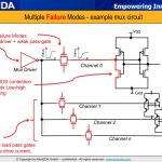
(3) gaining proper insight into how their circuit is behaving along with an understanding of failure … Read More
eSilicon ♥ ARM!
The things I enjoy the most at conferences are presentations by customers, the companies that solve the problems we face every day with modern semiconductor design. We all have access to the same tools and IP and use the same foundries so it’s the actual design and implementation that separates the wheat from the chaff, absolutely.… Read More


