When process nodes reached 28 nm and below, it appeared that design density is reaching a saturation point, hitting the limits of Moore’s law. I was of the opinion that the future of microelectronic physical design was limited to 20 and 14 nm being addressed by technological advances such as FinFETs, double patterning, HKMG (High-k… Read More
Tag: semi
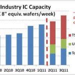
IC capacity utilization declined in 3Q 2011
SICAS (Semiconductor Industry Capacity Statistics) has released its 3Q 2011 data, available through the SIA at: SICAS data . Beginning with 2Q 2011 the SICAS membership list no longer includes the Taiwanese companies Nanya Technology, Taiwan Semiconductor Manufacturing Company Ltd. (TSMC) or United Microelectronics Corporation… Read More
Semiconductor equipment spending beginning to decline
Semiconductor manufacturing equipment shipments have leveled off after a strong rebound from the 2008-2009 downturn. August 2011 three-month-average shipments based on combined data from SEMI (North American and European companies) and SEAJ (Japanese companies) were $2.9 billion, down from a peak of $3.2 billion in May … Read More
Dawn at the OASIS, Dusk for GDSII
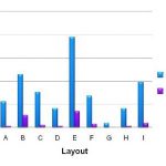
For an industry committed to constant innovation, changes in any part of the design flow are only slowly adopted, and only when absolutely necessary. Almost 10 years ago, it became clear that shrinking process technologies would bring a massive growth of layout and mask data—rougly 50% per node. This avalanche of data seriously… Read More


