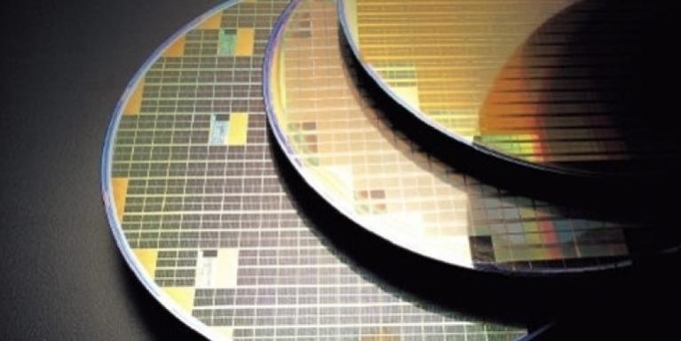
For Halloween this week we thought it would be appropriate to talk about things that strike fear into the hearts of semiconductor makers and process engineers toiling away in fabs. Do I want to do multi-patterning with the huge increase in complexity, number of steps, masks and tools or do I want to do EUV with unproven tools, unproven… Read More
Tag: samsung
Deal Struck for Sale of Toshiba NAND to Bain Apple and Others
What does it mean for the skyrocketing memory sector? In a last minute plot twist, Bain capital appears to be the winner in the auction of the Toshiba memory unit. The Bain consortium includes a strange cast of characters including Apple, Dell, Seagate, Kingston Technology, Innovation Network Corp of Japan and Development Bank… Read More
2017 Semiconductor Growth Approaching 20 Percent!
The 2017 semiconductor market is shaping up as the strongest since 2010 – when the market grew 32% as it bounced back from the 2008-2009 downturn. According to World Semiconductor Trades Statistics (WSTS), the second quarter 2017 semiconductor market was up 5.8% from 1Q 2017 and up 23.7% from a year ago. Much of the market vitality… Read More
Samsung, Synopsys and Qualcomm at DAC
I’m a user of many Samsung products as my family has Samsung Galaxy smart phones and my MacBook Pro uses Samsung SSD for storage, so at DAC I attended a breakfast panel with presenters from Samsung, Synopsys and Qualcomm. This was the second day of DAC and they served us breakfast, and with the big names on the panel the room was… Read More
AI ASICs Exposed!
Artificial intelligence, or AI is really heating up these days. The technology has been around for decades, but of late it is becoming quite a focus for applications such as data center analytics, autonomous vehicles and augmented reality. Why the rebirth? The trend appears to be driven by two forces – availability of data to train… Read More
Samsung Sloppy Sailor Spending Spree!
Last week, TEL (which is the Japanese equivalent to AMAT & LRCX) reported a June quarter which saw revenues drop to 236B Yen from March’s 261B Yen and saw earnings drop from March’s 47B Yen to June’s 41B Yen, a respective 9.3% decrease and a 12.8% decrease in earnings.
We don’t think this is attributable… Read More
Semicap Thoughts: ASML AMAT INTEL SAMSUNG TSMC MICRON
ASML reported results in line and slightly ahead of expectations which helped push ASML and the other semicap stocks back to their original valuations prior to the two step pull back that lasted about a month. We are now back to relatively high, record valuations not seen or ever seen previously (at least for a long time) by many companies.… Read More
Semicon West – The FDSOI Ecosystem
At Semicon West last week I attended presentations by Soitec and CEA Leti, and had breakfast with CEA Leti CEO Marie Semeria, key members of the Fully Depleted Silicon On Insulator (FDSOI) ecosystem. I have also seen some comments in the SemiWiki forum lately that make me believe there is some confusion on the roles of different companies… Read More
Standard Node Trend
I have previously published analysis’ converting leading edge logic processes to “standard nodes” and comparing standard nodes by company and time. Recently updated details on the 7nm process node have become available and in this article, I will revisit the standard node calculations and trends.… Read More
Exclusive – GLOBALFOUNDRIES discloses 7nm process detail
In a SemiWiki EXCLUSIVE – GLOBALFOUNDRIES has now disclosed the key metrics for their 7nm process. As I previously discussed in my 14nm, 16nm, 10nm and 7nm – What we know now blog GLOBALFOUNDRIES licensed their 14nm process from Samsung and decided to skip 10nm because they thought it would be a short-lived node. At … Read More


