You are currently viewing SemiWiki as a guest which gives you limited access to the site. To view blog comments and experience other SemiWiki features you must be a registered member. Registration is fast, simple, and absolutely free so please,
join our community today!
Reports of increasing TSMC 7NM lead times
There have been a number of increasing media reports about lengthening leads times for TSMC 7NM process. From what we have been able to determine its not due to TSMC having a yield bust or other production issues, it is simply one of stronger than expected demand.
There have been reports of … Read More
The IEEE International Electron Devices Meeting is in my opinion the leading technology conference to understand the current state-of-the-art in semiconductor process technology. Held each year in early December in San Francisco it is a must attend conference for anyone following technology development. The following is… Read More
Last year at Semicon I sat down with Soitec and got an update on the company. You can read my write up from last year here. A key point last year was Soitec was continuing to be profitable and grow after several years of financial struggles.
On Thursday, July 11th I got to sit down with Soitec’s CEO, Paul Boudre and get an update on… Read More
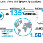
It seems every day we see a new article (or ten) on autonomous driving. It is an especially hot topic, and it will happen someday. For now, we can dream about it, and many people are working on it. But for the present, the technology in a car that commands my attention is audio. I’ve been a musician since 4th grade. I still perform occasionally… Read More
At the ES Design West event in San Francisco last week Silvaco’s CTO and EVP of Products, Babak Taheri, gave a presentation titled, “Next Generation SoC Design: From Atoms to Systems”. The time slot for the talk was only 30-minutes which is simply not enough to discuss all the technology Silvaco is providing now. I had not looked closely… Read More
2020 capex likely down at least 20% vs 2019 DRAM & NAND price drops versus slowing capacity. Investors happy cause it could have been worse.
Micron reported $1.05 in Non-GAAP EPS beating street consensus of $0.79 by $0.26. While this looks like a big beat, we would remind investors that estimates for the quarter were about… Read More
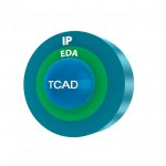
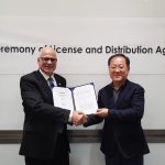
There were quite a few announcements at the Samsung Foundry Forum but my favorite was the IP partnership between Samsung and Silvaco. IP is a critical part of the fabless ecosystem and one of the advantages an IDM foundry has over a pure-play is the vast amounts of internal IP that have been silicon proven over the years. With Samsung… Read More
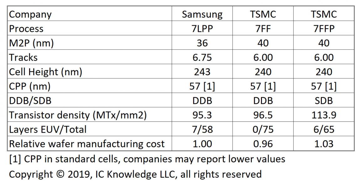
Samsung and TSMC have both made recent disclosures about their 5nm process and I though it would be a good time to look at what we know about them and compare the two processes.
A lot of what has been announced about 5nm is in comparison to 7nm so we will first review 7nm.
7nm
Figure 1 compares Samsung’s 7LPP process to TSMC’s 7FF and 7FFP… Read More
On the Sunday evening at IEDM last year, TechInsights held a reception in which Arabinda Das and Jeongdong Choe gave presentations that attracted a roomful of conference attendees.
This is the second part of the review of Jeongdong’s talk, we covered NAND flash technology in the last post. Jeongdong is a Senior Technical… Read More
TSMC and Samsung continue to raise the competitive bar for FinFET foundry market share with dueling announcements this week. As I mentioned previously in the blog Semiconductor Foundry Landscape Update 2019, FinFETs are the market to watch with the coming onslaught of 5G and AI chips on the edge, in the cloud, and in our autonomous… Read More