You are currently viewing SemiWiki as a guest which gives you limited access to the site. To view blog comments and experience other SemiWiki features you must be a registered member. Registration is fast, simple, and absolutely free so please,
join our community today!
Digital designers have used logic optimization and logic synthesis for decades as a means to produce more optimal designs with EDA tools. On the analog and transistor-level side of design the efforts to automatically optimize for speed or power have generally been limited to circuits with only a handful of transistors. These … Read More
Learning an HDL language or an HDL simulator are two different things, so I wanted to see what was available for learning a vendor-specific HDL simulator. I’ve already taught Verilog as an instructor using both ModelSim and Active-HDL simulators, however we only used a handful of commands in the class and labs in order to … Read More
Most IC engineers learn best by hands-on experience when another more experienced person can show us what to do. If you cannot find that experienced person, then the next best thing is a video from an expert. I was surprised to find out that video was so important today that the #2 most viewed web site on the Internet was www.youtube.com… Read More
IC designers use EDA tools to implement their logical and physical design, and these tools require foundry-specific information for:
- Design Rule Checking (DRC)
- Layout Versus Schematic (LVS)
- Library Symbols
- Parasitic EXtraction (PEX)
…
Read More
Dassault have recently been granted a patent on their approach to managing design hierarchy. I asked them how long it took from filing the patent until it was granted and they said the whole process had taken 8 years. It is a bit of an indictment of the patent system when it takes 8 years, also known as 4 or 5 process nodes, for a patent to… Read More
Last week I heard about the Indian Cabinet approving the proposal for setting up of two Fabs in India. One led by IBM, Tower Jazzand JP Associates(an Indian business house), and the other led by HSMC(Hindustan Semiconductor Manufacturing Co.), ST Microelectronicsand Silterra. Indian Semiconductor community including IESA… Read More
Lately I was studying about new innovations in memory world such as ReRAM and Memristor. As DRAM (although it has become a commodity) has found its extensive use in mobile, PC, tablet and so on, that was an inclination too to know more about. While reviewing Cadence’s offering in memory subsystems, I came across this whitepaperwhich… Read More
Remember? During DAC2013 I talked about a new kind of innovation: A Virtual Fabrication Platform, SEMulator3D, developed by COVENTOR. Now, to my pleasant surprise, there is something to report on the proven results from this platform. IBM, in association with COVENTOR, has successfully implemented a 3D Virtual Fabrication… Read More
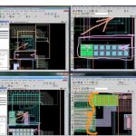
Layout editing is a complex task, traditionally done manually by designers, and the layout design productivity largely depends on the designer’s skills and expertise. However, a good tool with features for ease of design is a must. Layout productivity has been an area of focus and various features are constantly being added in… Read More
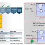
Here, I am talking about reliability of chip design in the context of electrical effects, not external factors like cosmic rays. So, the electrical factors that could affect reliability of chips could be excessive power dissipation, noise, EM (Electromigration), ESD (Electrostatic Discharge), substrate noise coupling and… Read More