You are currently viewing SemiWiki as a guest which gives you limited access to the site. To view blog comments and experience other SemiWiki features you must be a registered member. Registration is fast, simple, and absolutely free so please,
join our community today!
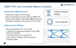
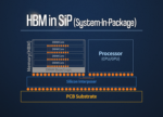
In the technology realm of artificial intelligence (AI) and high-performance computing (HPC), the demand for higher throughput and efficiency has never been greater. To meet these evolving demands, innovative memory solutions have emerged as critical enablers, paving the way for transformative advancements in computing… Read More
– AMAT slightly better than expected, flat & guides flat but > expected
– Expects better 2024- Systems flat, service up, display down
– China risk remains high at 45%- $200M Sculpta expected in 2024
– HBM 5% of industry but not a lot of tool sales- but high growth
Still bumping along with flattish … Read More
– Lam reported as expected and guided flat- No recovery yet
– Some mix shifts but China still 40% (8X US at 5%)-NVM still low
– HBM is promising but Lam needs a broad memory recovery
– Lam has not seen order surge ASML saw- Likely lagging by 3-4 QTRs
An in line quarter and uninspiring flat guide for Q1
As compared… Read More
-SEMICON well attended but bouncing along the biz bottom
-Recovery seems at least a year away with memory even more
-AI creates hope but not impactful- Disconnect tween stocks & reality
-AMAT me too platform- Back end benefits from chiplets
SEMICON busy but subdued
SEMICON is certainly back to pre-covid levels or perhaps better.… Read More
Often designers are amazed at the diversity of requirements fabricators and manufacturers have for metal filled areas in advanced package designs. Package fabricators and manufacturers do not like solid metal planes or large metal areas. Their strict metal fill requirements address two main issues. The dielectric and metal… Read More
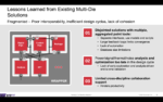
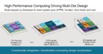
Multi-die design is not a new concept. It has been around for a long time and has evolved from 2D level integration on to 2.5D and then to full 3D level implementations. Multiple driving forces have led to this progression. Whether the forces are driven by market needs, product needs, manufacturing technology availability or EDA… Read More
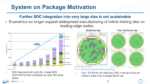
The foundry model, multi-source IP blocks, advanced packaging technologies, cloud computing, hyper-connectivity and access to open-source software have all contributed to the incredible electronics products of recent times. Along with this, the complexity of developing and taking a chip to market has also increased. And… Read More
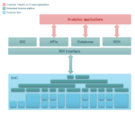
The move to true 3D IC, monolithic 3D SOC and 3D heterogeneous integration may require one of the most major design tool architecture overhauls since IC design tools were first developed. While we have been taking steps toward 3DIC with 2.5D designs with interposers, HBM, etc., the fundamental tools and flows remain intact in many… Read More
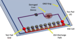
In the past ESD sign-off has been accomplished by a combination of techniques. Often ESD experts are asked to look at a design and assess its ESD robustness based on experience gained from prior chips. Alternatively, designers are told to work with a set of rules given to them, again based on previous experience about what usually… Read More
In early April, Gabriele Saucier kicked off Design & Reuse’s IPSoC Silicon Valley 2021 Conference. IPSoC conference as the name suggests is dedicated to semiconductor intellectual property (IP) and IP-based electronic systems. There were a number of excellent presentations at the conference. The presentations had been… Read More