You are currently viewing SemiWiki as a guest which gives you limited access to the site. To view blog comments and experience other SemiWiki features you must be a registered member. Registration is fast, simple, and absolutely free so please,
join our community today!
ASML- better EPS but weaker revenues- 2024 recovery on track
China jumps 10% to 49%- Memory looking better @59% of orders
Order lumpiness increases with ASP- EUV will be up-DUV down
“Passing Bottom” of what has been a long down cycle
Weak revenues & orders but OK EPS
Reported revenue was Euro5.3B and EPS of Euro3.11… Read More
The majority of EUV production is on 5nm and 3nm node, implemented by late 2022. Metal oxide resists have not been brought into volume production yet [1,2], meaning that only organic chemically amplified resists (CARs) have been used instead until now. These resists have a typical absorption coefficient of 5/um [3,4], which means
…
Read More
The discussion of any particular lithographic application often refers to imaging a single pitch, e.g., 30 nm pitch for a 5nm-family track metal scenario. However, it is always necessary to confirm the selected patterning techniques on the actual use case. The 7nm, 5nm, or 3nm 6-track cell has four minimum pitch tracks, flanked… Read More
– Lam reported as expected and guided flat- No recovery yet
– Some mix shifts but China still 40% (8X US at 5%)-NVM still low
– HBM is promising but Lam needs a broad memory recovery
– Lam has not seen order surge ASML saw- Likely lagging by 3-4 QTRs
An in line quarter and uninspiring flat guide for Q1
As compared… Read More
– ASML orders more than triple sequentially- Utilization increases
– Management remains conservative with flat revenues 2024 vs 2023
– Recovery will be slow, targeting 2025- Long & weak cyclical bottom
– Litho orders are leading indicator of future wider recovery
Strong orders pave the way for
…
Read More
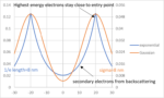
EUV lithography is a complicated process with many factors affecting the production of the final image. The EUV light itself doesn’t directly generate the images, but acts through secondary electrons which are released as a result of ionization by incoming EUV photons. Consequently, we need to be aware of the fluctuations… Read More
On a DRAM chip, the patterning of features outside the cell array can be just as challenging as those within the array itself. While the array contains features which are the most densely packed, at least they are regularly arranged. On the other hand, outside the array, the regularity is lost, but the in the most difficult cases, … Read More
In recent advanced nodes, via and cut patterning have constituted a larger and larger portion of the overall BEOL mask count. The advent of SALELE [1,2] caused mask count to increase for EUV as well, resulting in costs no longer being competitive with DUV down to 3nm [3]. Further development by TEL [4] has shown the possibility for… Read More
Electron beam lithography is commercially used to directly write submicron patterns onto advanced node masks. With the advent of EUV masks and nanometer-scale NIL (nanoimprint lithography), multi-beam writers are now being used, compensating the ultralow throughput of a single high-resolution electron beam with the use… Read More
- This past weeks over-reaction to Canon echoes the Sculpta Scare
- Nanoimprint has made huge strides but is still not at all competitive
- Shows basic lack of understanding of technology by some pundits
- Chip industry has been searching for alternatives that don’t exist
Much ado about nothing much…..
This past week we … Read More