Last year, about 40% of new smartphones included Near Field Communication (NFC). Analysts predict that by 2017 there will be 1 billion NFC enabled phones. Clearly, the use of NFC is ramping up because it can simplify aspects as diverse as communication, secure payments, user authentication, and retail loyalty programs for instance.… Read More

Tag: esd
Electrostatic Discharge analysis of FinFET technology
Sofics recently had the opportunity to characterize FinFET technology through cooperation with one of its customers. We analyzed the technology related to ESD and identified several challenges.… Read More
How Magwel is Tapping Tried and True Business Strategy in Targeting ESD

Often when a company starts out it takes a while for it to find the sweet spot in the marketplace. Very often it is feedback from existing customers and business success that can help point the way for small companies as they grow. This is just as true in EDA as it is in retailing or consumer products. For instance, Mentor Graphics, though… Read More
A Complete Simulation Platform for Mobile Systems

If we take an insight into the semiconductor industry, we can easily find that mobile systems are the main drivers of this industry. The Smartphone business has remained at the top since a good number of years. Although the Smartphone sales growth has started showing a sign of stagnation, it is still a main contributor with a solid… Read More
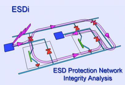
ESD Protection Network Checking is Difficult But Necessary
I’ve written before about anti-fuse non-volatile memory, where the gate oxide is intentionally damaged in order to create a readable bit of data, but this is what most circuit designers never want to have happen to their logic gates. However, since the advent of MOS transistors the issue of Electrostatic Discharge (ESD) and the… Read More
A Key Partner in the Semiconductor Ecosystem
Often we hear about isolated instances of excellence from various companies in the semiconductor industry which contribute significantly in building the overall ecosystem. While the individual excellence is essential, it’s rather more important how that excellence is utilized in a larger way by the industry to create a ‘value… Read More
Full-chip Multi-domain ESD Verification

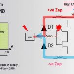
ESD stands for electro-static discharge and deals with the fact that chips have to survive in an electrically hostile environment: people, testers, assembly equipment, shipping tubes. All of these can carry electric charge that has the “potential” (ho-ho) to damage the chip irreversibly. Historically this was… Read More
SoCs More Vulnerable to ESD at Lower Nodes
Electro Static Discharge (ESD) has been a major cause of failures in electronic devices. As the electronic devices have moved towards high density SoCs accommodating ever increasing number of gates at lower process nodes, their vulnerability to ESD effects has only increased. Among the reasons for ESD failures in SoCs, device… Read More
FinFET Designs Need Early Reliability Analysis
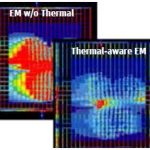
In a world with mobile and IoT devices driven by ultra-low power, high performance and small footprint transistors, FinFET based designs are ideal. FinFETs provide high current drive, low leakage and high device density. However, a FinFET transistor is more exposed to thermal issues, electro migration (EM), and electrostatic… Read More
Solution for PI, TI & SI Issues in 3D-ICs
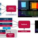
As we move towards packing more and more functionalities and increasing densities of SoCs, the power, thermal and signal integrity issues keep on rising. 3D-IC is a great concept to stack multiple dies on top of each other vertically. While it brings lot of avenues to package dies with multiple functions together, it has challenges… Read More