You are currently viewing SemiWiki as a guest which gives you limited access to the site. To view blog comments and experience other SemiWiki features you must be a registered member. Registration is fast, simple, and absolutely free so please,
join our community today!
Farm Managementby Paul McLellan on 03-01-2012 at 5:34 pmCategories: EDA
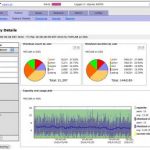
Every so often I come across a new company in EDA or one of its neighboring domains, new to me anyway, and new to SemiWiki. One such company is RunTime Design Automation (RTDA). They provide a suite of tools for managing server farms (or internal clouds which seems to be the trendy buzzword du jour). Running a few EDA scripts on a few servers… Read More
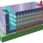
When process nodes reached 28 nm and below, it appeared that design density is reaching a saturation point, hitting the limits of Moore’s law. I was of the opinion that the future of microelectronic physical design was limited to 20 and 14 nm being addressed by technological advances such as FinFETs, double patterning, HKMG (High-k… Read More
Back in the Napoleonic era it was possible to manage a battle with very ad hoc methods. Sit on a horse on top of the highest hill and watch the battle unfold, send messengers out with instructions. By the First World War, never mind the second, that approach was hopelessly outdated and a much more structured way of managing a battle was… Read More
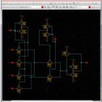
Digital designers have used diff tools for years on their text-based HDL source code, but what about for the transistor-level IC designer, where is their diff tool for schematics or layout?… Read More
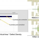
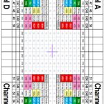
Although design for manufacturing (DFM) tools and techniques have been around for several nodes, a lot of designers remain skeptical about their actual value, especially since many products still make it successfully to market without the use of DFM.… Read More
DFM Industry Surveyby Beth Martin on 02-10-2012 at 1:28 pmCategories: EDA, Siemens EDA
As part of the DFM Conference at the SPIE Advance Lithography symposium, the DFM committee is conducting an informal survey on the current state of Design For Manufacturability in the Semiconductor Industry.
Please take this anonymous 16 question survey to identify critical Design for Manufacturability (DFM) issues facing… Read More
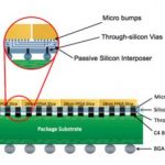
3D Standardsby Paul McLellan on 02-01-2012 at 5:06 pmCategories: Ansys, Inc., EDA
At DesignCon this week there was a panel on 3D standards organized by Si2. I also talked to Aveek Sarkar of Apache (a subsidiary of Ansys) who is one of the founding member companies of the Si2 Open3D Technical Advisory Board (TAB), along with Atrenta, Cadence, Fraunhofer Institute, Global Foundries, Intel, Invarian, Mentor, Qualcomm,… Read More
Next week there are two Apache, a subsidiary of Ansys, events. At DesignCon there are a couple of workshops on chip-package-system (CPS). In addition to Apache themselves, each of the two workshops has a number of representatives of leading edge companies doing semiconductor design. I already blogged about this in more detail… Read More
For the greater good of the semiconductor ecosystem, SemiWiki and Mentor Graphics present SemiWiki Seminars, a free seminar and software demonstration series addressing the latest innovations in IC design. SemiWiki Seminars discuss interesting new challenges and potential solutions aimed at increased circuit density … Read More
Looking at the huge gap between the revenue of semiconductor design and manufacturing (~$300B) and that of EDA tools, services and silicon IP combined (~6B) inspired me to look more deeply into the overall arena of semiconductors in today’s context and possibly decipher some trends which should emerge in near future. Although… Read More