You are currently viewing SemiWiki as a guest which gives you limited access to the site. To view blog comments and experience other SemiWiki features you must be a registered member. Registration is fast, simple, and absolutely free so please,
join our community today!
Yesterday Cadence had their annual front-end summit, the theme of which was physically aware design. I was especially interested in the first couple of presentations about physically aware synthesis. I joined Cadence in 1999 when they acquired Ambit Design Systems. One of the products that we had in development was called PKS… Read More
In an environment of SoCs with tough targets of multiple functionalities, smallest size, lowest power and fastest performance to achieve within a limited design cycle window in order to meet the rigid time-to-market requirements, any day spent without success becomes very frustrating for a designer. Especially during tape-out… Read More
The MOS-AK/GSA Modeling Working Group, a global compact modeling standardization forum, delivered its annual autumn compact modeling workshop on Sept. 20, 2013 as an integral part of the ESSDERC/ESSCIRC Conference in Bucharest (RO). The event received full sponsorship from leading industrial partners including Agilent… Read More
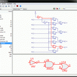
We cordially invite you to attend this webinar and learn how to quickly debug post layout designs. Concept Engineering is a privately held company based in Freiburg, Germany. It was, founded in 1990 to develop and market innovative schematic generation and viewing technology for use with logic synthesis, verification, test … Read More
There is always a lot of posturing and pontificating when semiconductor executives talk about the future of process development. They are fighting an air war of perception and investor expectations, so naturally want to make sure they have plenty to brag about. But, as we pointed out recently with Intel’s problems at 14nm, moving… Read More
Save closure time and boost performance by incorporating knowledge of physically aware design early into your front-end design implementation flow
With the adoption of advanced process nodes, design closure is becoming increasingly difficult due to the lack of convergence between the front end and the back end of the register-transfer… Read More
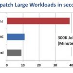
When you see a new product announcement from an EDA company, it is always put in terms that make it seem as if the engineer is sitting at his or her desktop with a big server and is running the new tool to wondrous effect. But the reality in the real world is that most companies have a computing infrastructure of server farms, often several… Read More
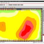
Yesterday Cadence had an all-day Signoff Summit where they talked about the tools that they have for signoff in advanced nodes. Well, of course, those tools work just fine in non-advanced nodes too, but at 20nm and 16nm there are FinFETs, double patterning, timing impacts from dummy metal fill, a gazillion corners to be analyzed… Read More
In the third and final (for now) part of this series on the EDA design tool vendors, I’d like to take a closer look at Cadence Design Systems. This is probably the most interesting of the three from both an industry perspective as well as an investment perspective for a variety of reasons. With that said I’d like to first provide some … Read More
eSilicon Corporation was founded in 2000 with Jack Harding as the founding CEO and Seth Neiman of Crosspoint Venture Partners as the first venture investor and outside Board member. They both remain involved in the company today, with Jack continuing as CEO and Seth now serving as Chairman of the Board.
Both Harding and Neiman brought… Read More