You are currently viewing SemiWiki as a guest which gives you limited access to the site. To view blog comments and experience other SemiWiki features you must be a registered member. Registration is fast, simple, and absolutely free so please,
join our community today!
-New PUV light source will push litho into Angstrom Era
-Rare earth elements shortages add to supply chain woes
-Could strategic wafer reserve releases lower memory pricing
-Can we cut off/turn off Russian access to chip equipment?
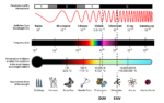
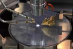
DUV, EUV and now “PUV” to become next generation lithography
Lithography is the locomotive… Read More
Lithography has been the driving force for shrinking feature sizes for decades, and the most easily identified factor behind this trend is the reduction of wavelength. G-line (436 nm wavelength) was used for 0.5 um in the late 1980s [1], and I-line (365 nm wavelength) was used down to 0.3 um in the 1990s [2]. Then began the era of deep-ultraviolet… Read More
– Strong demand across logic/memory & leading/trailing edge
– Customers want units fast-no time to test
– The main question is can ASML ramp to meet demand?
Revenue & Earnings low due to systems being rushed to customers
ASML reported Euro 4B in sales and Euro 1B in net income which while within guidance… Read More
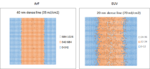
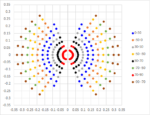
Due to the higher energy of EUV (13.3-13.7 nm wavelength) compared to ArF (193 nm wavelength) light, images produced by EUV are more susceptible to photon shot noise.
Figure 1. (Left) 40 nm dense (half-pitch) line image projected onto wafer at 35 mJ/cm2; (Right) 20 nm dense (half-pitch) line image projected onto wafer at 70 mJ/cm2.… Read More
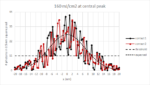
The stochastic behavior of images formed in EUV lithography has already been highlighted by a number of authors [1-3]. How serious it appears depends on the pixel size with which the photons are bunched. Generally, though, for features of around 20 nm or less, even 1 nm can have at least a +/- 15% gradient across it, which is still a
…
Read More
At the SPIE Advanced Lithography Conference held in February, ASML presented the latest information on their Deep Ultraviolet (DUV) and Extreme Ultraviolet (EUV) exposure systems. I recently got to interview Mike Lercel of ASML to discuss the presentations.
DUV
Despite all the attention EUV is getting, most layers are still… Read More
– ASML has good quarter driven by DUV & Logic (@72%)
– SMIC & other major customer slow EUV plans
– Logic (read that as TSMC) remains key demand led driver
– We are happy memory remains muted given cyclical potential
A very solid quarter with a continued road to growth
The quarter came in at Euro4,254B… Read More
- Covid related Revenue Rec causes rev/EPS miss
- Sharp order drop reflects H2 industry uncertainty
- EUV remains solid- Memory/Logic mix is better
Results were in line after correcting Covid Caused Revenue Rec issue-
ASML reported revenues of Euro3.3B and EPS of Euro1.79 as revenues from two EUV systems was not recognized, due to … Read More
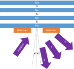
The stochastic nature of imaging has received a great deal of attention in the area of EUV lithography. The density of EUV photons reaching the wafer is low enough [1] that the natural variation in the number of photons arriving at a given location can give rise to a relatively large standard deviation.
In recent studies [2,3], it … Read More
EUV (Extreme UltraViolet) lithography has received attention within the semiconductor industry since its development inception in 1997 with the formation of the EUV LLC [1], and more recently, since the 7nm node began, with limited use by Samsung and TSMC being touted as key advantages [2, 3]. As with any key critical technology,
…
Read More