You are currently viewing SemiWiki as a guest which gives you limited access to the site. To view blog comments and experience other SemiWiki features you must be a registered member. Registration is fast, simple, and absolutely free so please,
join our community today!
State-of-the-art chips will always include some portions which are memory arrays, which also happen to be the densest portions of the chip. Arrayed features are the main targets for lithography evaluation, as the feature pitch is well-defined, and is directly linked to the cost scaling (more features per wafer) from generation… Read More
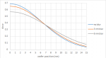
As any semiconductor process advances to the next generation or “node”, a sticky point is how to achieve the required higher resolution. As noted in another article [1], multipatterning (the required use of repeated patterning steps for a particular feature) has been practiced already for many years, and many have… Read More
EUV lithography is widely perceived to be the obvious choice to replace DUV lithography due to the shorter wavelength(s) used. However, there’s a devil in the details, or a catch if you will.
Electrons have the last word
The resist exposure is completed by the release of electrons following the absorption of the EUV photon.… Read More
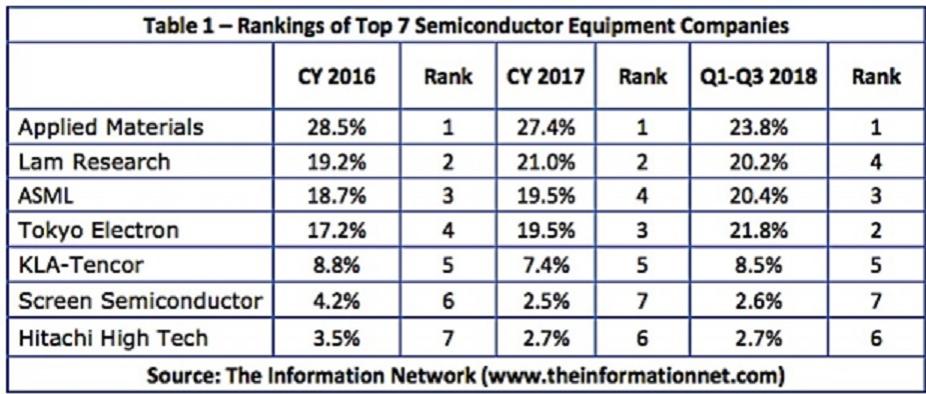
Semiconductor equipment vendor ranking, which didn’t change much between 2016 and 2017, is undergoing a makeover, as Lam Research, ASML, and Tokyo Electron (TEL) are switching places and top-ranked Applied Materials is getting closer to losing its number one ranking.
Since the 1990s, Applied Materials has been the market leader… Read More
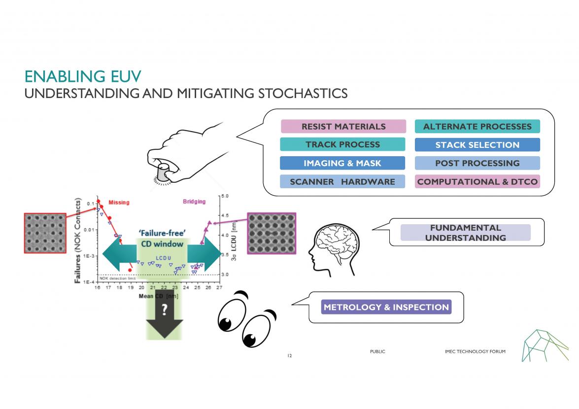
At SEMICON West I attended the imec technology forum, multiple Tech Spot presentations and conducted a number of interviews relevant to advanced lithography and EUV. In this article I will summarize what I learned plus make some comments on the outlook for EUV.… Read More