Casper van Oosten is the Business Field Head and Managing Director for Intermolecular, Inc., acquired by Merck KGaA, Darmstadt, Germany in 2019. Prior to this role, Casper worked in various roles on Eyrise™ Dynamic Liquid Crystal Window in Veldhoven, the Netherlands, at an affiliate of Merck KGaA, Darmstadt, Germany. Casper… Read More
Tag: dram
Will EUV take a Breather in 2021?
-KLAC- Solid QTR & Guide but flat 2021 outlook
-Display down & more memory mix
-KLAC has very solid Dec Qtr & guide but 2021 looks flattish
-Mix shift to memory doesn’t help- Display weakness
-Despite flat still looking at double digit growth
-EUV driven business may see some slowing from digestion
As always, … Read More
China Semiconductor Bond Bust!
– Tsinghua $198M Bond Bust
– Good for memory: Samsung Micron LG Toshiba –
– Not good for chip equipment
– Could China Credit Crunch hit more than foundry embargo?
– Damage to China memory positive for other memory makers
– Not good for chip equip if customers can’t get money
China’s… Read More
2021 will be the year of DRAM!
2020 has been a NAND growth year-2021 will be the year of DRAM. While foundry logic has gotten all the credit in 2020 the reality is that NAND has been up 2X in 2020 for semiconductor equipment provider Applied Materials (AMAT). It is expected that NAND will be flat in 2021 while DRAM will take over the growth slot with foundry/logic … Read More
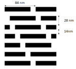
Application-Specific Lithography: a 28 nm Pitch DRAM Active Area
In the recent DRAM jargon, “1X”, “1Y”, “1Z”, etc. have been used to express all the sub-20 nm process generations. It is almost possible now to match them to real numbers which are roughly the half-pitch of the DRAM active area, such as 1X=18, 1Y ~ 17, etc. At this rate, 14 nm is somewhere around
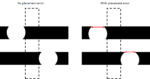
Reliable Line Cutting for Spacer-based Patterning
Spacer-defined patterning is an expected requirement for advanced semiconductor patterning nodes with feature sizes of 25 nm or less. As the required gaps between features go well below the lithography tool’s resolution limit, the use of cut exposures to separate features is used more often, especially in chips produced… Read More
LithoVision – Economics in the 3D Era
Each year on the Sunday before the SPIE Advanced Lithography Conference, Nikon holds their LithoVision event. This year I had the privilege of being invited to speak for the third consecutive year, unfortunately, the event had to be canceled due to concerns over the COVID-19 virus but by the time the event was canceled I had already… Read More
Minimal Corona Impact on Chip Equipment Stocks
Very solid quarter driven by foundry/logic
AMAT reported a very solid quarter, beating the top end of guidance with foundry and logic being the primary drivers of spend. Revenues were $4.16B and EPS of $0.98 non-GAAP versus street of $4.11B and $0.93 EPS.
Guide not too wide… – $300M “Corona Cut”
More importantly,… Read More
Logic and Memory Make for a Recovery
- LAM- “Logic And Memory” make for a recovery-NAND (Samsung) & Logic (TSMC) + China
- Great Q4 Results & Q1 guide as memory restarts
- Logic strength continues-China is crucial to growth
- 2019 better than expected- 2020 WFE up about 5-8%
Lam reports nice finish to 2019 and start of 2020
The company reported revenues… Read More
Could TSMC’s spend be part of the seasonal pattern?
Is there more downside than upside in stocks?
Entering a seasonally weak period, then what?
Does China trade come back to haunt industry?
Cycle is past the bottom-But what kind of up cycle?
The most recent up cycle in the industry was a huge one, driven by a huge spend on NAND as SSD’s sucked up infinite number of devices. DRAM … Read More