DAC starts in San Francisco on June 8th. The kickoff keynote at 9.20am that morning is by Brian Otis of Google. He is a director at Google[x]. According to Wikipedia:Google X, stylized as Google[x], is a semi-secret facility run by Google dedicated to making major technological advancements. It is located about a half mile from … Read More

Tag: dac
SoCs More Vulnerable to ESD at Lower Nodes
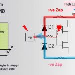
Electro Static Discharge (ESD) has been a major cause of failures in electronic devices. As the electronic devices have moved towards high density SoCs accommodating ever increasing number of gates at lower process nodes, their vulnerability to ESD effects has only increased. Among the reasons for ESD failures in SoCs, device… Read More
DAC: March Update
DAC is coming up. It is already March. If you are in the EDA industry then it is basically three months away, which sounds a lot until you actually have to get everything pulled together so that your booth is ready to go on Monday June 7[SUP]th[/SUP]. Exhibit hours have been extended and now run from 10am to 7pm (only until 6pm on Wednesday).… Read More
In-Design DFM Signoff for 14nm FinFET Designs
While FinFET yield controversy is going on, I see a lot being done to improve that yield by various means. One prime trend today, it must be, it’s worthwhile, is to pull up various signoffs as early as possible during the design cycle. And DFM signoff is a must with respect to yield of fabrication. This reminds me about my patents filed… Read More
DAC Deadlines: Action This Day
DAC is coming up. OK, it’s not actually until next June. It is June 7-11th 2015 at the Moscone Center here in San Francisco. But there are lots of important deadlines coming up for papers, panels and more. The 52[SUP]nd[/SUP] DAC will focus on five key tracks:
- automotive
- IP design
- embedded systems
- hardware/software security
Key Collaboration to Enable Designs at Advanced Nodes
In the semiconductor ecosystem, several partners (or better to say stakeholders) join together in the overall value chain to finally output the most coveted chip, err I should say SoC these days. It becomes really interesting when we start analyzing the real value added by each of them, none appears to be less. Well, then to whom … Read More
IP and Design Management Done Right

At DACin San Francisco this past June I was able to visit and blog about two dozen EDA companies, however there were so many more products and events to see that I couldn’t possibly have enough time to enjoy them all. Fortunately for me there were plenty of videos made of vendor presentations, so this week I got caught up a bit by… Read More
Samsung 14nm FinFET Design with Cadence Tools
The first consumer products with 20nm processing are arriving in 2014 like the 2 billion transistor A8 chip in the iPhone 6, however at the 14nm node there are new designs underway to continue the trend of Moore’s Law. To get a better feel for the challenges of designing with 14nm FinFET technology I watched a 23 minute video … Read More
Automatic RTL Restructuring: A Need Rather Than Convenience
In the semiconductor design industry, most of the designs are created and optimized at the RTL level, mainly through home grown scripts or manual methods. As there can be several iterations in optimizing the hierarchy for physical implementation, it’s too late to do the hierarchical optimizations after reaching the floor plan… Read More
Crossfire – Your partner for IP development, what’s new?
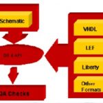
As the SoCs and IPs grow in sizes and complexities, the number of formats, databases, libraries of standard cells and IOs also increase. It becomes a clumsy task to check every cell in a library, its consistency among various format with respect to functionality, timing, naming, labels and so on, and its complex physical properties… Read More