You are currently viewing SemiWiki as a guest which gives you limited access to the site. To view blog comments and experience other SemiWiki features you must be a registered member. Registration is fast, simple, and absolutely free so please,
join our community today!
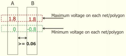
Because IC design and verification never gets simpler, verification engineers now have to comply with voltage-dependent DRC (VD-DRC) rules. What does this term mean, and what new challenges does it bring to the DRC task? I’d like to share what I learned during another water-cooler conversation with Dina Medhat, senior technical… Read More
I was talking recently to Dina Medhat, a senior technical marketing engineer at Mentor, about, of all things, IO rings. It has not occurred to me that verifying that your IO rings comply with foundry rules presents new challenges.
IO ring checking isn’t new, nor is it unique to advanced IC process nodes. However, the same forces of… Read More
It’s less than four weeks to go at DAC 2015 and the program is final now. So I started investigating new technologies, trends, methodologies, and tools that will be unveiled and discussed in this DAC. In the hindsight of the semiconductor industry over the last year, I see 14nm technologies in the realization stage and 10nm beckoning… Read More
Mentor Graphics made a big announcement regarding SOC extraction at their User2User conference in San Jose during April. Before I get to the meat of the announcement, I’d like to reflect back on the early days of Calibre-DRC at Mentor. I was in Sales at Mentor around 1999, and Calibre-DRC was the new kid on the block. We had to go convince… Read More
Almost anyone that is active in IC design will be “in touch” with Electrostatic Discharge (ESD) at some time (pun intended). Preventing ESD related IC failures remains something like black magic—at least it’s easy to get that feeling when you are trying to debug ESD failures. I/O and ESD layouts that resulted in excellent robustness… Read More
Yesterday Mentor announced their quarterly results. Since their financial year is not aligned with the calendar year, this was also the end of their fiscal 2015. The quarter was an all-time record with revenues of $439M and (non-GAAP) EPS of $1.09. The year was also an all-time record with revenues of $1.24B and EPS of $1.77. Half… Read More
Place & route in the 16/14nm era requires a new approach since it is significantly more complex. Of course, every process generation is more complex than the one before and the designs are bigger. But modern processes have new problems. The two biggest changes are FinFETs and double patterning.
FinFETs, as I assume you know,… Read More
In my career in semiconductor industry, I can recall, in the beginning there was emphasis on design completion with automation as fast as possible. The primary considerations were area and speed of completion of a semiconductor design. Today, with unprecedented increase in multiple functions on the same chip and density of the… Read More
Even though I live just 7 miles away from the Mentor Graphics corporate office in Oregon, I visited their DAC suite in San Francisco last week to get an update on Calibrefrom Michael White. The Calibre tools are used during IC verification and sign-off by performing DRC (Design Rule Checking) and LVS (Layout Versus Schematic).… Read More
I think by now a lot has been said about the necessity of multi-patterning at advanced technology nodes with extremely low feature size such as 20nm, because lithography using 193nm wavelength of light makes printing and manufacturing of semiconductor design very difficult. The multi-patterning is a novel semiconductor manufacturing… Read More