You are currently viewing SemiWiki as a guest which gives you limited access to the site. To view blog comments and experience other SemiWiki features you must be a registered member. Registration is fast, simple, and absolutely free so please,
join our community today!
TowerJazzis a specialty foundry that provides IC manufacturing into several markets, like: RF, high-performance analog, power, imaging, consumer, automotive, medical, industrial and aerospace/defense. In June there was a presentation from Ofer Tamir of TowerJazz at DACin the Cadence theatre, so I had a chance this week … Read More
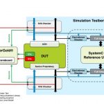
The Jasper part of Cadence announced jointly with Sonics a relationship whereby Sonics uses JasperGold Apps as part of their verification. I talked to Drew Wingard, the CTO, about how they use it.
One way is during the day when their design engineers use Jasper as part of their verification arsenal. Interestingly it is the design… Read More
Semiconductor Safetyby Daniel Nenni on 11-06-2014 at 7:00 amCategories: Cadence, EDA
Semiconductors and automotive are now like peanut butter and jelly. Certainly you can have one without the other but why would you? I remember when a car first talked to me telling me that the door was ajar. It sounded more like, “the door is a jar” but I got the point. Now my car tells me just about everything including what is wrong with… Read More
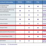
While FinFET yield controversy is going on, I see a lot being done to improve that yield by various means. One prime trend today, it must be, it’s worthwhile, is to pull up various signoffs as early as possible during the design cycle. And DFM signoff is a must with respect to yield of fabrication. This reminds me about my patents filed… Read More
Will you go to Grenoble next week to attend to IP-SoC? I will do it and will certainly listen to these Keynote Talks:
…
Read More
Yesterday was Cadence’s annual mixed-signal technology forum. I think that there was a definite theme running through many of the presentations, namely that wireless communication of one kind or another is on a sharp rise with more and more devices needing to connect to WiFi, Bluetooth and so on. This was most obvious during… Read More
I first visited STat their Agrate, Italy site where Flash memory development is done. At DACthis year Antonio Bogani talked about how ST designs with LDE while using EDA tools and a PDK (Process Design Kit) from Cadence. They recorded the 17 minute presentation, and you can view it herewithout having to register. Antonio’s… Read More
TSMC ♥ Cadence!by Daniel Nenni on 10-11-2014 at 4:30 pmCategories: Cadence, EDA, IP, TSMC
One of the questions I routinely ask amongst the fabless semiconductor ecosystem is, “How are the EDA vendors doing?” There are always complaints because, let’s face it, we all like to complain. On occasion however I do hear about a vendor who goes above and beyond the call of duty and it really brightens my day.
Of late,… Read More
In the semiconductor ecosystem, several partners (or better to say stakeholders) join together in the overall value chain to finally output the most coveted chip, err I should say SoC these days. It becomes really interesting when we start analyzing the real value added by each of them, none appears to be less. Well, then to whom … Read More
Whoever has said that history never repeats itself should read this recent PR from AMD! The news can be summarized in three points:
- Multi-year agreement gives AMD access to a range of Synopsys design IP including interface, memory compiler, logic library and analog IP for advanced FinFET process nodes
- Synopsys acquires rights
…
Read More