In modern electronic industry PCBs are required to accommodate highly dense circuits with large number of components and complex routing spaces. While the complexity is increasing, the time-to-market is decreasing. In such a scenario, there is no other option than to reduce the design time by employing innovative editing options… Read More
Tag: cadence
SemiWiki at #52DAC: Nominated for Best Paper Award!
Blogging for Semiwiki is a very good exercise to prepare a paper submission at DAC. Writing a short article using about 600 words to pass one message, and try to deliver this message as clearly as possible. Writing a paper for DAC is very similar, as you have to be synthetic and develop a thesis in 5 slides, no more, as it’s a time limited… Read More
Feed Your Mind and Body at 52nd DAC!
My beautiful wife and I attend the Design Automation Conference together whenever possible. More so now that she is the co-founder and CFO of SemiWiki. It is really nice for her to put a face to the invoices and personally thank our subscribers. Her first DAC was 1985 in Las Vegas. We were married for less than a year so it was like a second… Read More
TSMC 10nm Readiness and 3DIC
At the TSMC Technology Symposium last month Suk Lee presented a lot of information on design enablement. Suk is an interesting guy with a unique background in ASIC, Semiconductor, EDA, and now Foundry. In baseball terms that would be like playing infield, outfield, home plate, and umpire!
Around the turn of the millennium Suk actually… Read More
SoC Debugging Just Got a Speed Boost
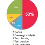
Sure, design engineers can get more attention than verification engineers, but the greater number of verification engineers on SoC projects means that the verification task is a bigger bottleneck in a schedule than pure design work. A recent survey conducted at Cadence shows how verification effort can be divided into several,… Read More
Growing Innovation in Modern PCB Design Tools
In last 30+ years, the electronic design industry has seen rapid changes more than any other industry. The change has taken place in the whole electronic ecosystem including semiconductor technology, transistor design, IC / SoC design, PCB, and system design. Today, a PCB can be very complex connecting several heterogeneous… Read More
SystemC Co-Simulation of NoCs and IP Blocks
Verification in general suffers from a couple of fundamental problems. Availability of models and performance of different levels of representation.
The first problem, availability of models, is that you would like to start verification as soon as possible but all the representations are not ready early enough. Obviously … Read More
ARM & Cadence IP Partnership for Faster SoC Design
IP vendors always try to create differentiation, especially when designing protocol based IP. You can differentiate by building the most performing controller but you will probably miss the expectation of these customers who don’t search for performance but just compliance to a specific standard. Or the vendor may want to design… Read More
Cadence’s New Implementation System Promises Better TAT and PPA
On Tuesday Cadence made a big announcement about their new physical implementation offering, Innovus, during the keynote address at the CDNLive event in Silicon Valley. Cadence CEO Lip-Bu Tan alluded to it during his kick off talk, and next up Anirudh Devgan, Senior Vice President, Digital & Signoff Group, filled in more … Read More
Innovus: Cadence’s Next Generation Implementation System
Yesterday was the first day of CDNLive. There were three keynotes. The first was by Lip-Bu Tan, Cadence’s CEO (and the Chairman of Walden International that he will be the first to remind you). The most interesting tidbit was that Cadence now has over 1000 people working on IP and that it represents 11% of their revenue. Then… Read More


