You are currently viewing SemiWiki as a guest which gives you limited access to the site. To view blog comments and experience other SemiWiki features you must be a registered member. Registration is fast, simple, and absolutely free so please,
join our community today!
With over 18 years of experience in the semiconductor industry, Rodrigo Jaramillo is the Co-Founder and CEO of Circuify Semiconductors, an engineering design solutions startup based in Guadalajara, Mexico. Circuify provides ASIC, SoC, and Chiplet design services for the North American semiconductor industry, with experience… Read More
Custom and Analog-Mixed Signal (AMS) IC design are used when the highest performance is required, and using digital standard cells just won’t meet the requirements. Manually sizing schematics, doing IC layout, extracting parasitics, then measuring the performance only to go back and continue iterating is a long, tedious… Read More
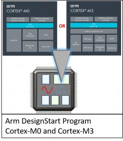
For SOC designers that are waiting for library models the saying “give me liberty or give me death” is especially apropos. Without libraries to support the timing flow, SOC design progress can grind to a halt. As is often the case, more than just a few PVT corners are needed. Years ago, corners were what the term sounded like – the 4 corners… Read More
Sometimes the hardest thing about bringing a new idea to fruition is overcoming the inertia to get started with a proof-of-concept. You must be able to put together enough parts of the solution to prove to those controlling budgets that an idea has merit and is worth taking to the next level. It’s a bit of a chick-vs-egg scenario as … Read More
There are three critical goals that designers of custom digital designs and memories look to achieve with high sigma verification:
(1) obtaining accurate results,
(2) achieving results with good run-time (efficiency), and
(3) gaining proper insight into how their circuit is behaving along with an understanding of failure … Read More
In recent years, a number of technologies as well as the constant desire for faster and more pervasive mobile communication systems have set in motion a well sustained growth trend for the “next big thing” such as the Internet of Things (IoT), wearables, automobile electronics, advances in medical devices etc. In all these areas… Read More
You have to love when a professional journalist leaks a story and cites a “source close to the acquisition.” News flash: Anyone “close” to the acquisition is under NDA which is a legally binding agreement, not very professional if you ask me. Bloggers however can write whatever they want but since I was actually “close” to … Read More
High-capacity IC place and route (P&R) tools can cost $200K and more to own from the big three vendors (Cadence, Synopsys, Mentor), but what about IC designs that are primarily Big Analog and Little Digital? In the EDA world we often have multiple choices for tools, and there are affordable alternatives to place and route out… Read More
Most analog cells have a power off mode intended to reduce power consumption. In this mode, all the circuit branches between the supply lines are set in a high impedance mode by driving MOS gates to a blocking voltage. This is a somewhat similar situation to that in tri-state digital circuits.
When a branch is set in that high impedance… Read More
There has been a lot written on this topic, and some expensive tools proposed to solve this issue, but it is still a concern and a mystery for many designers. The point is that whatever efforts you do, the substrate is common to an entire chip and can cause some undesired coupling if not managed properly and at an early stage. As a start… Read More