You are currently viewing SemiWiki as a guest which gives you limited access to the site. To view blog comments and experience other SemiWiki features you must be a registered member. Registration is fast, simple, and absolutely free so please,
join our community today!
I was asked to give a talk at the 2021 ISS conference and the following is a write up of the talk.
The title of the talk is “Logic Leadership in the PPAC era”.
The talk is broken up into three main sections:
- Background information explaining PPAC and Standard Cells.
- A node-by-node comparisons of companies running leading edge logic
…
Read More
As semiconductor designs for many popular products move into smaller process nodes, the need for effective and rapid design closure is increasing. The SOCs used for many consumer and industrial applications are moving to FinFET nodes from 16 to 7nm and with that comes greater challenges in obtaining design closure. einfochips,… Read More
Seeking Alpha just published an article about Intel and Samsung passing TSMC for process leadership. The Intel part seems to be a theme with them, they have talked in the past about how Intel does bigger density improvements with each generation than the foundries but forget that the foundries are doing 5 nodes in the time it takes… Read More
I have seen several articles recently discussing foundry wafer selling prices for leading edge wafers, these articles all quote estimates from a paper by the Center for Security and Emerging Technology (CSET). The paper is available here.
My company IC Knowledge LLC is the world leader in cost and price modeling of semiconductors… Read More
While Alchip is speeding its way down the TSMC process technology roadmap I am reminded how important services are to the semiconductor ecosystem. We can thank ASIC companies like Alchip for the heavy investment systems companies have made into semiconductors. We covered this in our book “Fabless: The Transformation of the Semiconductor… Read More
At SEMICON West, Applied Materials announced a new selective gap fill tool to address the growing resistance issues in interconnect at small dimensions. I had the opportunity to discuss this new tool and the applications for it with Zhebo Chen global product manager in the Metal Deposition Products group at Applied Materials.… Read More
Summary
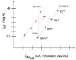
As a result of extensive focus on the development of workfunction metal (WFM) deposition, lithography, and removal, both FinFET and gate-all-around (GAA) devices will offer a wide range of Vt levels for advanced process nodes below 7nm.
Introduction
Cell library and IP designers rely on the availability of nFET and pFET… Read More
I have written a lot of articles looking at leading edge processes and comparing the process density. One comment I often get are that the process density numbers I present do not correlate with the actual transistor density on released products. A lot of people want to draw conclusions an Intel’s processes versus TSMC’s processes… Read More
Recently Seeking Alpha published an article “Taiwan Semiconductor Manufacturing Company Losing Its Process Leadership To Intel” and Dan Nenni (SemiWiki founder) asked me to take a look at the article and do my own analysis. This is a subject I have followed and published on for many years.
Before I dig into specific process density… Read More
I couldn’t attend the SPIE Advanced Lithography Conference this year for personal reasons, but last week Mike Lercel of ASML was nice enough to walk me through the major ASML presentations from the conference.
Introduction
In late 2018, Samsung and TSMC introduced 7nm foundry logic processes with 5 to 7 EUV layers, throughout … Read More


