You are currently viewing SemiWiki as a guest which gives you limited access to the site. To view blog comments and experience other SemiWiki features you must be a registered member. Registration is fast, simple, and absolutely free so please,
join our community today!
The semiconductor industry has built decades of success on hyper-integration to increase functionality and performance while also reducing system cost. But the standard way to do this, to jam more and more functionality onto a single die, breaks down when some of the functions you want to integrate are built in different processes.… Read More
The Death of Moore’s Lawby Michael Barger on 01-22-2016 at 12:00 pmCategories: EDA
For the last several years, people have predicted the end of Moore’s Law. The reasoning is that there is a limit at which one can’t shrink transistors any further. A reoccurring comment has been “You can’t divide an atom.” I had assumed that its demise would be at the hands of a new paradigm like quantum computing. Now, with Intel’s … Read More
At the TSMC Technology Symposium last month Suk Lee presented a lot of information on design enablement. Suk is an interesting guy with a unique background in ASIC, Semiconductor, EDA, and now Foundry. In baseball terms that would be like playing infield, outfield, home plate, and umpire!
Around the turn of the millennium Suk actually… Read More
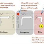
The use of silicon interposers is growing. Several years ago Xilinx broke new ground by employing interposers in their Virtex®-7 H580T FPGA. Last August Samsung announced what they say is the first DDR4 module to use 3D TSV’s for enterprise servers. Their 64GB double data rate-4 modules will be used for high end computing where … Read More
EDPS: Fins and FinFETsby Paul McLellan on 04-02-2015 at 7:00 amCategories: EDA
Look at those dolphins with fins on their backs. Did you know that FinFETs are actually named after them since Chenming Hu and his team though that they looked like a fish’s fin? And since they invented FinFETs they got to name them too. But those dolphins also mean that it is nearly time for this years Electronic Design Process… Read More
More news from the 3DASIP conference. Chet Palesko of SavanSys Solution had an interesting presentation with the same title as this blog (although this blog draws from several other presentations too). Chet took a look at what aspects of 3D are likely to get cheaper going forward. He took as a starting point that stuff that is not … Read More
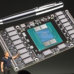
I have been at the 3D ASIP conference that is held every year in Burlingame. It is far and away the best place to get a snapshot on what is going on in 3D (and 2.5D) IC design each year. One of the presentations was by the guys from Yole on where the industry is right now. Other presentations were on pathfinding, power reduction (did you know… Read More
3DIC in Burlingameby Paul McLellan on 12-01-2014 at 7:00 amCategories: Events
Every year in December is what I think of as the main 3D IC conference where you can get up to speed on all the latest. Officially it is called 3D Architectures for Semiconductor and Packaging or 3D ASIP. It is held in the Hyatt Regency in Burlingame (the one right by 101 near the airport). This year it is from December 10-12th.
The first… Read More
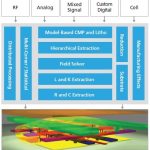
Last month Cadenceannounced its fastest parasitic extraction tool (minimum 5 times better performance compared to other available tools) which can handle growing design sizes with interconnect explosion, number of parasitics and complexities at advanced process nodes including FinFETs, without impacting accuracy of … Read More
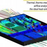
Last week my daughter was playing some games on my Google Nexus smartphone for a while when one of my friends called. When I picked up the phone, I couldn’t imagine it was so hot. There is no doubt; every electronic device today emits an order of magnitude higher heat than what it used to at most a decade ago. There is so much emphasis on … Read More