You are currently viewing SemiWiki as a guest which gives you limited access to the site. To view blog comments and experience other SemiWiki features you must be a registered member. Registration is fast, simple, and absolutely free so please,
join our community today!
Establishing void-free fill of high aspect ratio TSVs, capped by a thin and uniform bulk layer optimized for removal by CMP, means fully optimizing each of a series of critical phases. As we will see in this 3-part series, the conditions governing outcomes for each phase vary greatly, and the complexity of interacting factors means… Read More
In today’s rapidly advancing technological landscape, semiconductors are at the heart of innovation across diverse industries such as automotive, healthcare, telecommunications, and consumer electronics. As a leader in technology and engineering, Siemens plays a pivotal role in empowering the next generation … Read More
In today’s rapidly evolving semiconductor industry, the design and integration of intellectual property (IP) play a pivotal role in achieving competitive advantage and market success. Whether sourced from commercial IP providers or developed in-house, ensuring that IP designs are compliant with signoff requirements… Read More
While the leap from traditional SoC/IC designs to Three-Dimensional Integrated Circuits (3DICs) designs brings new benefits and opportunities, it also introduces new challenges. The benefits include performance, power efficiency, footprint reduction and cost savings. The challenges span design, verification, thermal… Read More
As we all know, hearing directly from the people who actually use EDA tools, people who are solving real world problems with the latest technologies are the best source of information. Thus EDA User group meetings are always first on my event list every year which brings us to Ansys Ideas.
Ansys User Group Meeting Features Technical
…
Read More
At the recent Synopsys Users Group Meeting (SNUG) I had the honor of leading a panel of experts on the topic of chiplets. One of those panelists was the very personable Dr. Henry Sheng, Group Director of R&D in the EDA Group at Synopsys. Henry currently leads engineering for 3DIC, advanced technology and visualization.
Are we
…
Read More
One of my favorite events is just around the corner and that is the TSMC OIP Ecosystem Forum and it’s at my favorite Silicon Valley venue the Santa Clara Convention Center. Nobody knows more about the inner workings of the ecosystem than TSMC so this is the premier semiconductor collaboration event, absolutely.
In my 40 years as a … Read More
There is a major shift in innovation occurring all around us. We see the results every day. We can interact with them in an easier, more intuitive way. They deliver insights about our health and our daily habits. All this can be categorized as a move towards Smart Everything – ubiquitous machine-assisted intelligence for the good… Read More
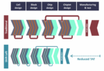
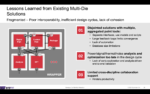
Multi-die design is not a new concept. It has been around for a long time and has evolved from 2D level integration on to 2.5D and then to full 3D level implementations. Multiple driving forces have led to this progression. Whether the forces are driven by market needs, product needs, manufacturing technology availability or EDA… Read More
The introduction of direct die-to-die bonding technology into high volume production has the potential to substantially affect the evolution of the microelectronics industry. The concerns relative to the “end of Moore’s Law”, the diminishing returns of continued (monolithic) CMOS process scaling, and the disruptive effect… Read More