You are currently viewing SemiWiki as a guest which gives you limited access to the site. To view blog comments and experience other SemiWiki features you must be a registered member. Registration is fast, simple, and absolutely free so please,
join our community today!
Kinam Kim is a longtime Samsung technologist who has published many excellent articles over the years. He is now the Chairman of Samsung Electronics, and he gave a very interesting keynote address at IEDM.
He began with some general observations:
The world is experiencing a transformation powered by semiconductors that has been… Read More
At the 2021 VLSI Technology Symposium, Imec presented on Ruthenium (Ru) and Molybdenum (Mo) as alternate Word Line (WL) materials for 3D NAND Flash “First Demonstration of Ruthenium and Molybdenum Word lines Integrated into 40nm Pitch 3D NAND Memory Devices”. I had an opportunity to interview one of the authors: Maarten Rosmeulen.… Read More
There are a lot of articles out right now discussing a possible IPO for Kioxia or sale of the company with Western Digital (WD) and Micron Technology (MT) mentioned as possible acquirers. Kioxia and WD have a partnership for Flash Memory and on March 18th WD gave a presentation on the state of their partnership and what they see as their… Read More
Casper van Oosten is the Business Field Head and Managing Director for Intermolecular, Inc., acquired by Merck KGaA, Darmstadt, Germany in 2019. Prior to this role, Casper worked in various roles on Eyrise™ Dynamic Liquid Crystal Window in Veldhoven, the Netherlands, at an affiliate of Merck KGaA, Darmstadt, Germany. Casper… Read More
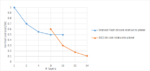
I recently posted an insightful article [1] published in 2013 on the cost of 3D NAND Flash by Dr. Andrew Walker, which has since received over 10,000 views on LinkedIn. The highlight was the plot of cost vs. the number of layers showing a minimum cost for some layer number, dependent on the etch sidewall angle. In this article, the same… Read More
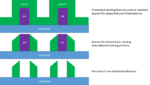
Toshiba (now known as Kioxia) was the first company to propose a 3D stacked version of NAND Flash memory called BICS [1]. BICS (BIt Cost Scalable) Flash used explicit process cost reduction based on depositing and etching multiple layers at once, avoiding multiple lithography steps. This strategy replaced the usual approach… Read More
Nonvolatile memory capacity reached 64 Gb levels when NAND Flash half-pitch reached 20 nm [1]. Having reached 14 nm [2], NAND Flash half-pitch is no longer being reduced, now that it has entered the 3D era. However, recently, 3D XPoint has found applications within the Optane platform [3]. The lithography for patterning 20 nm half-pitch… Read More
Each year on the Sunday before the SPIE Advanced Lithography Conference, Nikon holds their LithoVision event. This year I had the privilege of being invited to speak for the third consecutive year, unfortunately, the event had to be canceled due to concerns over the COVID-19 virus but by the time the event was canceled I had already… Read More
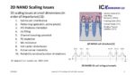
In order to beat Moore’s Law NAND Flash memories have moved from a planar topology to 3D construction. This allows for increased memory sized in much the same way a multistory building provides more building square footage on the same size building lot. Just like in building construction, adding a third dimension to the mix increases… Read More
Flash memory has become ubiquitous, so much so that it is easy to forget what life before it was like. Large scale non-volatile storage was limited spinning disks, which were bulky, power hungry and unreliable. With NAND Flash, we have become used to carrying many gigabytes around with us all the time in the form of cell phones, USB… Read More