Flash memory has become ubiquitous, so much so that it is easy to forget what life before it was like. Large scale non-volatile storage was limited spinning disks, which were bulky, power hungry and unreliable. With NAND Flash, we have become used to carrying many gigabytes around with us all the time in the form of cell phones, USB… Read More

Tag: 3d nand
Semicon West was sluggish with hopes of 2020 recovery
Bouncing along a not too bad bottom
Given that we have followed the semiconductor industry through many down cycles, we can safely say that this one isn’t all that bad by comparison. Everyone, big & small, is still safely profitable and in relatively good shape. Though we are seeing the normal week long holiday shut downs
LithoVision 2019 – Semiconductor Technology Trends and their impact on Lithography
I was asked to present at Nikon’s LithoVision event again this year. LithoVision is held the day before the SPIE Advanced Lithography Conference also in San Jose. The following is a write up of my talk.… Read More
Semiconductor Metrology Inspection Outpacing Overall Equipment Market in 2018
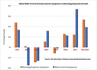
As uncertainties mount about the near-term semiconductor industry from companies in Apple’s supply chain and the significant drop in memory chip prices, the semiconductor industry has consistently grown each year since the great recession of 2009. Semiconductor revenues have consistently outpaced semiconductor equipment… Read More
The Disconnect Between Semiconductor and Semiconductor Equipment Revenues
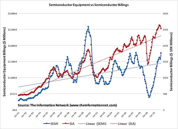
Historically, the semiconductor and semiconductor equipment industry were inextricably linked due to the cyclical nature of the chip industry. An increase in semiconductor revenues was followed within a short period with an increase in equipment revenues, as semiconductor companies purchased equipment to make more chips… Read More
Imec technology forum 2018 – the future of memory
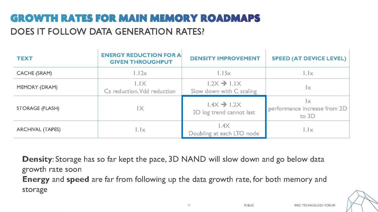
At the Imec technology forum in Belgium Gouri Sankar Kar and Arnaud Furnemont presented memory and storage perspectives and I also got to interview Arnaud. Arnaud leads overall memory development at Imec and personally leads NAND and DNA research.
Memory research is focused on power, energy, speed and cost with energy and throughput… Read More
Cleaning Trends for Advanced Nodes
I was invited to give a talk at the Business of Cleans Conference held by Linx Consulting in Boston on April 9th. I am not a cleans expert but rather was invited more to give an overview talk on process technology trends and the impact on cleans. In this write up I will discuss my presentation. I discussed each of the three main leading-edge… Read More
LithoVision 2018 The Evolving Semiconductor Technology Landscape and What it Means for Lithography
I was invited to present at Nikon’s LithoVision event held the day before the SPIE Advanced Lithography Conference in San Jose. The following is a write up of the talk I gave. In this talk I discuss the three main segments in the semiconductor industry, NAND, DRAM and Logic and how technology transitions will affect lithography.… Read More
Samsung Sloppy Sailor Spending Spree!
Last week, TEL (which is the Japanese equivalent to AMAT & LRCX) reported a June quarter which saw revenues drop to 236B Yen from March’s 261B Yen and saw earnings drop from March’s 47B Yen to June’s 41B Yen, a respective 9.3% decrease and a 12.8% decrease in earnings.
We don’t think this is attributable… Read More
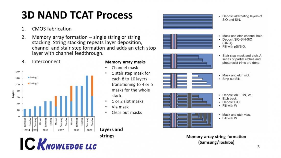
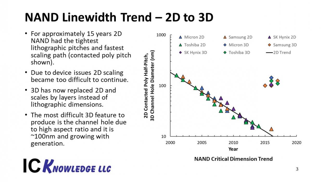
3D NAND Myths and Realities
For many year 2D NAND drove lithography for the semiconductor industry with the smallest printed dimensions and yearly shrinks. As 2D NAND shrunk down to the mid-teens nodes, 16nm, 15nm and even 14nm, the cells became so small that there were only a few electrons in each cell and cross-talk issues made further shrinks very difficult… Read More