You are currently viewing SemiWiki as a guest which gives you limited access to the site. To view blog comments and experience other SemiWiki features you must be a registered member. Registration is fast, simple, and absolutely free so please,
join our community today!
Over its 40+ year history, electronic design automation (EDA) has seen many companies rise, fall, and merge. In the beginning, in the 1980s, the industry was dominated by what came to be known as the big three — Daisy Systems, Mentor Graphics, and Valid Logic (the infamous “DMV”). The Big 3 has morphed over the years, eventually settling… Read More
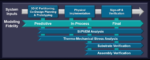
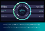
An earlier blog started with the topic of delivering 3D IC innovations faster. The blog covered the following foundational enablers for successful heterogeneous 3D IC implementation.
- System Co-Optimization (STCO) approach
- Transition from design-based to systems-based optimization
- Expanding the supply chain and tool
…
Read More
3D IC technology development started many years ago well before the slowing down of Moore’s law benefits became a topic of discussion. The technology was originally leveraged for stacking functional blocks with high-bandwidth buses between them. Memory manufacturers and other IDMs were the ones to typically leverage this … Read More
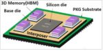
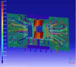
3D-ICs bring together multiple silicon dies into a single package that’s significantly larger and complex than traditional systems on a chip (SoCs). There’s no doubt these innovative designs are revolutionizing the semiconductor industry.
3D-ICs offer a variety of performance advantages over traditional SoCs. Because … Read More
Semiconductor manufacturers are under constantly increasing and intense pressure to accelerate innovative new chip designs to market faster than ever in smaller package sizes while assuring signal integrity and reducing power consumption. Three-dimensional integrated circuits (3D-ICs) promise to answer all these demands… Read More
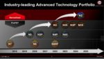
The TSMC Technical Symposium is today so I wanted to give you a brief summary of what was presented. Tom Dillinger will do a more technical review as he has done in the past. I don’t want to steal his thunder but here is what I think are the key takeaways. First a brief history lesson.
The history of TSMC Technology Development with 12 key… Read More
For the past few decades, System-on-Chip (SoC) has been the gold standard for optimizing the performance and cost of electronic systems. Pulling together practically all of a smartphone’s digital and analog capabilities into a monolithic chip, the mobile application processor serves as a near-perfect example of an SoC. But… Read More
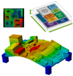
Our smart phones, tablets, laptops and desktops are the most common consumer products with advanced 2.5D and 3D IC packaging techniques. I love seeing the product tear down articles to learn how advanced packaging techniques are being used, so at the User2User conference in Santa Clara I attended a presentation from Tarek Ramadan,… Read More
It was nice to be at a live conference again. DesignCon was held at the Santa Clara Convention Center, my favorite location, which to me there was a back to normal crowd. The sessions I attended were full and the show floor was busy. Masks and vaccinations were not required, maybe that was it. Or there was a pent-up demand to get back engaged… Read More
The incredible growth that the semiconductor industry has enjoyed over the last several decades is attributed to Moore’s Law. While no one argues that point, there is also industry wide acknowledgment that Moore’s Law started slowing down around the 7nm process node. While die-size reductions still scale, performance jumps… Read More