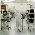
Intel’s investor meeting was held yesterday and for me the presentation that is most interesting is Bill Holt’s. The presentations are available on the Intel website: Intel Corporation – Presentations Material 2014. Here is the 2013 version of this presentation: Intel Corporation – Presentations Materials 2013… Read More

Tag: 10nm
Global Foundries and IBM, More Details
Now that the dust has started to settle on the GlobalFoundries acquisition of IBM’s semiconductor business it is possible to look into another level of detail about what GlobalFoundries will be acquiring in the way of technology and IP. Of course, the deal hasn’t formally closed yet so this won’t all happen … Read More
IEDM 2014 Preview
The International Electron Devices Meeting (IEDM) is one of the premier conferences for the presentation of the latest semiconductor processes and process technologies. IEDM is held every year in December alternating between San Francisco and Washington DC. This year IEDM will be held at the San Francisco Hilton on December… Read More
Imec and Coventor Partner Up
Today imec and Coventor announced a joint development project for 10nm and 7nm process development. Imec, which is in Leuven Belgium, is a partner with pretty much all the semiconductor companies that are planning work at these advanced nodes. It mostly does pre-competitive research and development. This type of research is … Read More
Cliff Hou at TSMC OIP
I attended Cliff Hou’s keynote at TSMC OIP Forum earlier this month. OIP is a huge undertaking. It currently has over 100 ecosystem partners, 10 technology generations, 7600+ IPs, 60+ EDA tools, 7000+ tech files and 150+ PDKs.
Most of Cliff’s presentation gave details on where TSMC are with the various processes. … Read More
10nm, the View from IBM
On the Cadence booth at DAC, Lars Liebmann of IBM presented on the challenges of 10nm. As he put it, how the lithography folks are keeping things very interesting for the EDA tool development engineers. Although 14nm/16nm hasn’t yet ramped into HVM, the advanced work for tools and IP has all moved to 10nm. Although Lars gave… Read More
The Apple Samsung TSMC Intel 14nm Mashup!
One of the strengths of the fabless semiconductor ecosystem is competition since it keeps innovation high and prices low. One of the challenges of fostering competition is that you have to make good on a threat of using a competing product during a pricing negotiation. Well, in my opinion, for the next version of the iPhone, Apple… Read More
ANSYS Tools Shine at FinFET Nodes!
In the modern semiconductor ecosystem we are seeing rapid advancement in technology breaking past once perceived limits; 28nm, 20nm, 16-14nm, 10nm and we are foreseeing 7nm now. Double and multi-patterning are already being seen along with complex FinFET structures in transistors to gain the ultimate advantages in PPA from… Read More
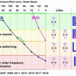
Who Will Lead at 10nm?
There has been a lot of discussion on SemiWiki lately around 14nm FinFET technology and who really leads and by how much. I thought it would be interesting to review some process metrics for previous technology generation and then make some forecasts around 10nm.
The focus of this article will be Intel, TSMC and Global Foundries/Samsung… Read More
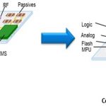
Samsung Foundry Explained!
Rather than watch the World Cup battle for third place, my beautiful wife and I spent last Saturday afternoon at the CASPA Wearables Symposium. The most interesting presentation was from Samsung because it included slides on their foundry offering. In regards to wearables, I still don’t see the ROI I need to buy one, yet. We are getting… Read More