You are currently viewing SemiWiki as a guest which gives you limited access to the site. To view blog comments and experience other SemiWiki features you must be a registered member. Registration is fast, simple, and absolutely free so please,
join our community today!
I spent all of last week at SEMICON West meeting with customers, potential customers, partners and various industry analysts and experts. I was involved in many interesting discussions over the course of the week and I thought I would share some of the more interesting observations:
Alternate Fin Materials Pushed Out
I have for… Read More
Cliff Hou had two major appearances at DAC this year. He gave the opening day keynote…and he wrote the forward to Dan and my bookFabless: the Transformation of the Semiconductor Industry which about 1500 lucky people got a copy of courtesy of several companies, most notably eSilicon who sponsored the Tuesday evening post-conference… Read More
At the SEMI ISS conference earlier this week, the last speaker in the technology challenges section was Handel Jones of IBS. I’ve known Handel since the mid-1980s when he came to VLSI Technology and told us we were losing money on 90% of the designs we were doing but our cost model was not good enough and so we didn’t even… Read More
At major EDA events, CEDA (the IEEE council on EDA, I guess you already know what that bit stands for) hosts a lunch and presentation for attendees and others. This week was ICCAD and the speaker was Lars Liebmann of IBM on The Escalating Design Impact of Resolution-Challenged Lithography. Lars decided to give us a whirlwind tour … Read More
It is beginning to look as if 28nm transistors, which are the cheapest per million gates compared to any earlier process such as 45nm, may also be the cheapest per million gates compared to any later process such as 20nm.
What we know so far: FinFET seems to be difficult technology because of the 3D structure and so the novel manufacturing… Read More
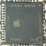
As a semiconductor professional and an Apple customer I’m very interested to see what is inside the iPhone5s. Rumors are spreading, photos are leaking, creating a nice build up to the next release of the mobile device that changed the world.
Honestly, last year I was a bit disappointed with the iPhone5. Inside is the A6 SoC which uses… Read More
Yesterday was the 2013 GSA Silicon Summit, which was largely focused on contrasting what advances in delivering systems will depend on marching down the ladder of process nodes, and which will depend on innovations in packaging technology. So essentially contrasting Moore’s Law with what has come to be known as More Than… Read More
Cliff Hou of TSMC gave the keynote today at SNUG on Collaborate to Innovate: a Foundry’s Perspective. Starting around 45nm the way that a foundry has to work with its ecosystem fundamentally changed. Up until then, each process generation was similar enough to the previous one, apart obviously from size, that it could be … Read More
At DAC 2012 we were hearing about the 20nm design ecosystem viability, however IC process technology never stands still so we have early process development going on now at the 10nm and 14nm nodes where FinFET technology is being touted. Earlier in February Vassilios Gerousis, a distinguished engineer at Cadence presented a session… Read More
As you know, I’ve been a bit of a bear about what is happening to wafer costs at 20nm and below. At the Common Platform Technology Forum last week there were a number of people talking about this in presentations and at Harvey Jones’s “fireside chat”.
At the press lunch I asked about this. There are obviously… Read More