Sondrel is an interesting and unique company. They are a supplier of turnkey services from system to silicon supply. So far, not that unique as there are a lot of companies with this mission. What is unique is their focus on complex designs. The company takes on the design of chips that would need teams of engineers working for a year with the aim of providing economy of scale. I’ve spent some time at the leading edge of custom chip design, and I can tell you it’s not for the faint of heart. This stuff is very, very difficult and those that can help are rare and quite valuable. There are lots of ways to address the daunting challenges of complex custom chip design, so I was quite excited to be able to get some of the backstory from a key member of the Sondrel team. Read on to learn how Sondrel explains one of the secrets of its success – NoC design.
First, some of the basics. If you want to learn more about his unique company, you can read an in-depth interview Daniel Nenni did with Sondrel’s CEO here. Next a bit about a NoC, or network on chip technology. If you think of typical IP building blocks for an SoC as the electrical fixtures in a home, the NoC is the wiring. It’s the interconnect backbone that delivers the right data to the right location at the speed required to make the whole system work. Doing something as complex as interconnecting the elements in an SoC, and even beyond to the external devices such as memory really benefits from a structured approach. That’s what a NoC delivers. This technology can offer the margin of victory if done correctly.
I was able to catch up with Dr. Anne-Françoise Brenton, Sondrel’s NoC expert. Anne-Françoise has extensive design experience from ST Micro, Thomson Consumer Electronics and Thomson Multi-Media, and TI before joining Sondrel over seven years ago. Anne-Françoise offered some great insights into why a NoC is so critical to complex chip design and how Sondrel approaches its design.
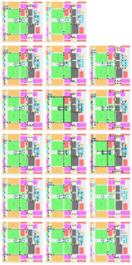
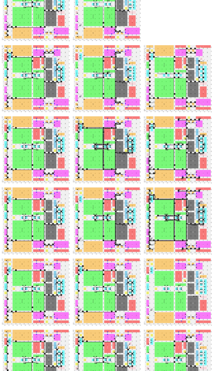
She began by explaining that in an ideal design all the sections that need high speed, high data flow between them would be located as close together as possible. That is, memory in the middle of the chip next to the blocks of IP that need memory access. In reality, apart from cache, memory is located off chip on dedicated memory chips, which use state-of-the-art memory technologies so that access points to memory are located on the perimeter of the chip. As a result, a complex network of interconnections is needed to route the data traffic between blocks and to and from off-chip memory. On a big chip design, there could be seventeen layers of horizontal interconnections plus a number of vertical connections between these layers. The graphic at the top of this post illustrates such a case.
In her words, “It’s rather like designing a massive, multi-level office block where you have to design it to allow for optimal movement of people between areas and floors. Where a lot of people need to move rapidly between two locations, you need a wide fast corridor and the length of it affects the timing of the arrival of people. Similarly, an infrequently used, non-urgent route can be long and narrow, and therefore slow. The analogy continues with the vertical interconnects being lifts with big capacity, lifts that just connect two specific floors to provide a dedicated route for high-speed connections, and lifts that stop at all floors that are slower but connect a lot of locations. On top of this is the arbitration that dynamically controls the data flow through the NoC with buffering to smooth and optimize as demand changes, for example when two IP blocks are sharing and accessing the same memory.”
Is your head hurting yet? Mine was. Anne-Françoise went on to explain that designing a NoC is an iterative collaboration throughout the entire chip design process between the front end, back end and NoC teams of designers.
She went on to explain that one of the challenges in NoC design is that third party IP blocks can be a black box solution with very little data provided on its demands for data flow as the vendor wants to protect the exact workings of its IP. This is actually overcome as the whole design matures by using timing analysis performance modeling to help ensure that the NoC is delivering the data as required by arbitrating the pathways to deliver the data according to pre-assigned priorities – there cannot be any bottlenecks.
Anne-Françoise concluded our discussion by explaining that “NoC design is a constantly changing juggling act. Change one parameter and several other things could change. It’s as intellectually challenging as playing several games of chess simultaneously and it is immensely rewarding.”
The holistic perspective that Anne-Françoise offered was quite refreshing. Sondrel seems to have its act together when tackling near-impossible high-end design. If you need help doing the impossible, I would strongly recommend you contact Sondrel, now that you’ve seen how Sondrel explains one of the secrets of its success – NoC design. You can learn more about Sondrel here.
Also Read:
SoC Application Usecase Capture For System Architecture Exploration
CEO interview: Graham Curren of Sondrel
Sondrel explains the 10 steps to model and design a complex SoC
Share this post via:


Comments
There are no comments yet.
You must register or log in to view/post comments.