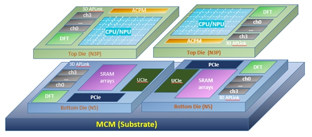
Today Alchip Technologies, a Taipei-based leader in high-performance and AI computing ASICs, announced a significant milestone with the successful tape-out of its 3D IC test chip. This achievement not only validates Alchip’s advanced 3D IC ecosystem but also positions the company as a frontrunner in the rapidly evolving field of three-dimensional integrated circuits. By proving the readiness of an integrated 3DIC solution, including critical components like CPU/NPU cores, UCIe and PCIe PHY, Lite-IO infrastructure, and third-party IP, Alchip is paving the way for faster, more efficient designs in artificial intelligence (AI) and high-performance computing (HPC).
The importance of this test chip lies in its validation of Alchip’s comprehensive 3DIC ecosystem, which is tailored to meet the demands of complex ASIC designs. Unlike traditional 2D ICs, 3DICs involve stacking multiple dies vertically, introducing unique challenges in power density, thermal dissipation, and interconnectivity. Alchip’s test chip, integrating a 3nm top die and a 5nm base die using TSMC’s SoIC-X packaging technology, was designed to tackle these challenges head-on. The successful tape-out confirms the company’s ability to deliver a robust design flow, die-to-die IP, and interconnect solutions, ensuring accuracy and reduced time-to-market for AI and HPC developers.
“What these test chip results should tell hyperscalers and other AI/HPC designers is that don’t have to settle for less-than design-optimal advanced packaging solutions. We’ve just proven an advanced packaging ecosystem that can meet the most precise 3DIC requirements,” explained Dr. Dave Hwang, Sr. Vice President and North America General Manager, Alchip Technologies.
A key aspect of the test chip is its demonstration of advanced 3DIC capabilities. The top die incorporates a CPU, NPU core, and high-power logic, while the base die features a network-on-chip, L3 cache, and interface IP. These components are connected via APLink-3D Lite IO, enabling seamless communication between dies. The tape-out validated critical features, including cross-die synchronous IP, design-for-test strategies with redundancy and repair, signal and power integrity analysis, thermal and mechanical simulations, and 3D physical design implementation. These validations are crucial, as 3DIC designs require precise coordination to ensure performance and reliability across stacked dies.
Alchip’s achievement is particularly noteworthy due to the complexity of 3DIC design. Unlike 2D counterparts, 3DICs demand new approaches to physical and logical integration. Alchip updated its electronic design automation (EDA) tools and methodologies to support co-design across both dies, ensuring electrical, timing, and mechanical integrity. The company also tested custom interface IP tailored for 3DICs, addressing interoperability challenges for protocols like UCIe and PCIe. A standout feature is the 3DI/O timing, which limits die-to-die latency to just 40 picoseconds. This low latency, combined with a fully integrated 3D clocking structure, minimizes timing skew and ensures coherent operation across layers, a critical factor for high-performance applications.
The test chip program also highlighted Alchip’s collaborative approach. Four IP vendors participated, with two providing proven hard macros and two others testing new IP on the platform. An EDA flow vendor ensured tool and methodology readiness, reinforcing the ecosystem’s strength. This collaboration underscores the scarcity of 3DIC-proven IP, making Alchip’s validated solutions highly valuable for developers seeking reliable components for next-generation ASICs.
The implications of this tape-out extend beyond the test chip itself. By stress-testing power density and thermal dissipation, Alchip has gathered insights that will inform future 3DIC designs, including those using TSMC N2, N3 and N5 stacked chiplets.
Bottom line: Alchip’s 3DIC test chip tape-out marks a pivotal moment for the semiconductor industry. By validating its 3DIC ecosystem, Alchip not only demonstrates technical prowess but also provides a reliable pathway for AI and HPC innovation. This milestone sets a new standard for 3DIC design, promising faster, more efficient, and scalable solutions for the future of computing.
The official news release is here.
About Alchip
Alchip Technologies Ltd., founded in 2003 and headquartered in Taipei, Taiwan, is a leading global High-Performance Computing and AI infrastructure ASIC provider of IC and packaging design, and production services for system companies developing complex and high-volume ASICs and SoCs. Alchip provides faster time-to-market and cost-effective solutions for SoC design at mainstream and advanced process technology. Alchip has built its reputation as a high-performance ASIC leader through its advanced 2.5D/3D CoWoS packaging, chiplet design, and manufacturing management. Customers include global leaders in artificial intelligence, high-performance computing, supercomputing, mobile communications, entertainment devices, networking equipment, and other electronic product categories.
Also Read:
Alchip Launches 2nm Design Platform for HPC and AI ASICs, Eyes TSMC N2 and A16 Roadmap
Alchip’s Technology and Global Talent Strategy Deliver Record Growth
Alchip is Paving the Way to Future 3D Design Innovation
Share this post via:


Comments
There are no comments yet.
You must register or log in to view/post comments.