Here are the Top 10 highlights from the recent TSMC 2018 Technology Symposium, held in Santa Clara CA. A couple of years ago, TSMC acknowledged the unique requirements of 4 different market segments, which has since guided their process development strategy — Mobile, High-Performance Computing (HPC), Automotive, and IoT. Many of the highlights described below are in the context of a specific platform.
(11) Bonus
The process development roadmap at TSMC has been extremely aggressive over the past few years — in large part, driven by product release schedules from a key customer or two. As a result, there have been numerous advanced process nodes introduced.
Even TSMC acknowledges that a subset of the offerings (with platform-specific variants) will be the key “long-life” nodes — e.g., 28nm, 16/12nm, and 7nm. Yet, on several occasions, TSMC stressed how the other nodes have provided critical “learning”.
Although the number of customer tapeouts (and any ongoing process improvement initiatives) for N20SoC and N10FF weren’t highlighted at the symposium, the learning that these nodes provided was mentioned. “The fab capacity for N10 will directly transition to N7, with the same equipment. The defect density learning at N10 has resulted in the fastest D0 transition at N7 for any node ever.”
(10) TSMC’s market growth outlook is extremely robust.
TSMC is increasing their R&D and cap equip investments substantially year-over-year, in anticipation of significant growth in: Artificial Intelligence/Machine Learning acceleration products, 5G wireless communications/infrastructure, and Automotive MCU and sensor electronics.
“The amount of data traffic associated with the transition from 4G-LTE to 5G will exceed 50% CAGR through 2020.”, B.J. Woo, VP of Business Development, highlighted. “Both the Mobile and HPC data center server markets will grow significantly — AI assist/acceleration and 5G will be big technology drivers.”
Dr. Kevin Zhang, VP, Business Development, also shared some interesting forecasts for the IoT market segments. “This past year, there were 800M wearable units sold, 2.5Bu for the smart home, 1.3Bu for the smart city, and 1.6Bu for industrial IoT applications. In the overall IoT area, there will be a 24% CAGR, with 6.2Bu sold in 2022.”
R&D investment increase of 20% YoY, from $2.07B to $2.6B, with an R&D headcount increase from 5,423 to 6,145. CapEx will increase from $10.9B in 2017 to $11.5-12B in 2018.
One of the more interesting graphs presented drew a parallel between the growth of the semi market and the growth of the global GDP, the implication being that semiconductor products have helped facilitate the worldwide growth of economic output. An interesting analogy, I thought.

(9) The 2018 investment in increased wafer capacity for advanced nodes is substantial.
The current 2017 capacity is 11M 12″ equivalent wafers. This will increase ~9% to 12M equivalent 12″ wafers annually by year-end 2018.
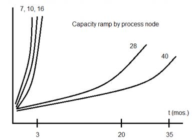
Roughly 35% of current capacity is available for N10, N16, N20, and N28, with an estimated 30% CAGR capacity demand. (Wow!) The graph below illustrates the (actual and planned) capacity ramp by node over time – it’s pretty amazing how much the demand profile has changed.
Another 35% of capacity is used for 40nm through 90nm. The remaining 30% corresponds to the 8″ fabs at 180nm and 230nm.
There are three “GigaFabs” being used for advanced process nodes, Fab 12, Fab 15, and Fab 18. Fabs 15 and 18 have “multi-phase” expansion plans — typically 6-7 phases each, adding ~50K wpm capacity per phase.
The status of the newer fabs is:
- Fab 15 is in production for N10, and the N7 ramp. (Phase 7 is currently under construction.) The expectation is a run rate of 1.1M wafers annually for N7 in 2019.
- Fab 18 phases 1-3 are underway, for the N5 ramp in 2020.
- Fab 16 is located in Nanjing China, with phases 1 and 2 targeting ~40K wpm each for N16.
TSMC is definitely not anticipating any slowdown in the logic (and specialty) semi market for the foreseeable future.
(8) R&D emphasis
The advanced R&D discussion introduced some novel technology development work underway.
“Nanosheets” are likely to emerge as the replacement to FinFET devices. Source/drain carrier tunneling and reduced electrostatic control will necessitate pursuing alternative transistor technologies to FinFET’s at the 3nm node. Additional “single-layer, two-dimensional” electron device carrier materials are being researched — e.g. MoS2.
Significant process R&D is focused on increasing metal grain size for interconnects — e.g., 10X grain size to reduce R (by ~50%!) and improve EM reliability.
There was also a distinct emphasis on RF technology development, to provide a potential front-end module solution that would incorporate a Low-Noise Amplifier (LNA) and Power Amplifier (PA) for upcoming 5G networks — e.g., N22ULP-RF and N16FFC-RF.
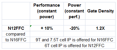
(7) N16FFC and N12FFC
There’s lot of activity to qualify 16FFC for the Automotive platform — specifically, there is a new “aging flow” introduced.
“The first automotive product in N16FFC is in production, with more than 10 customers actively engaged.”
There are some unique characteristics to the N12FFC process migration — a “dual metal pitch” BEOL definition is available (in support of legacy IP, I would surmise).
And, a new “5V LDMOS” device for I/O’s is available, to simplify the design of I/O interfaces at 1.5-1.8V (eliminating the need for series cascode devices to manage the higher VDDIO voltage).
Over 220 customer tapeouts in N16FFC/N12FFC are anticipated in 2018.
(6) N28HPC+, and the migration to N22ULP/ULL
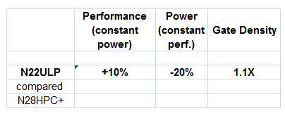
Just when you thought that “half-node” process introductions were no longer feasible, TSMC has introduced a shrink of N28HPC+ designs, to a node interestingly called “N22ULP” (same design rules as N28HPC+).
“We have over 50 customers and 140 tapeouts in N22ULP, spanning many application areas… connectivity, Digital TV/STB, application processors.”
An additional N22ULL (ultra low leakage) node will be introduced, with two specific features — an eHVT device, and a 0.6V VDD enablement (for “foundation IP”). The N22ULL SRAM Vmin remains at the nominal VDD of 0.8V for N22, necessitating a dual-rail supply strategy with arrays at 0.8V and logic at 0.6V.
(5) N7
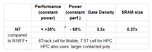
Process node N7 is in volume production, with >50 customer tapeouts expected by YE’18.
Although the initial target was the Mobile platform, there is an N7 variant developed specifically for HPC. A new 7.5 track SC library was developed (versus 6T for Mobile_. The N7 HPC option also includes a larger contacted poly pitch and wider metals, and a new “super high-density” MIM capacitor.
“We’re working on the N7 enablement for the Automotive platform as well — N7 should be qualified for automotive applications by 2Q19.” (Grade 1 application, I think, but I’m not sure.)
(4) N7+
This variant of N7 introduces EUV “selectively” — as an example, the SEM photos shown at the symposium highlighted the replacement of multipatterning via masks with a single EUV exposure.
There were lots of positive comments on the status of EUV lithography:
- improvements in sustained output power, at 145W since the start of 2018, with 250W demonstrated
- newer resist sensitivity has improved
- pellicle transmissivity is currently at 83%, with a goal of 90% in 2019
- the CD uniformity is exceptional, compared to 193i
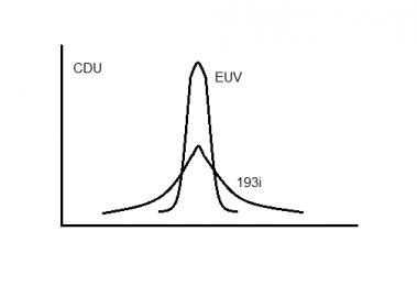
The N7+ rules offer a tighter metal pitch, which has some ramifications on transitioning an existing design from N7. A new set of standard cell IP is required, and new cell-based block composition would be needed.
TSMC is anticipating “risk production” status for N7+ in 3Q18. (The reliability qualification is underway — there were charts presented that highlighted qual data for: SRAM VCC_min drift after stress, ESD robustness for HBM and CDM tests, HTOL, etc.)

(4) N5, and “analog density” ?
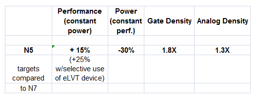
The N5 node is “full-fledged” EUV — by “full-fledged”, TSMC implied the mask count would be reduced by ~30% over N7. (They did not provide specific details.)
Early adopters will have access to a v0.5 PDK in June. IP developed for the v0.1 PDK is available for early adopters, with v0.5 PDK-based IP available in July.
The EDA tool support for N5 early adopters will require a multi-EDA vendor investment, as the flow enablement matrix is still evolving at Cadence, Mentor, Synopsys, and Ansys.
For the first time (to my recollection), TSMC has introduced a new term when comparing the PPA of different process nodes — i.e.,“analog density”. Alas, there wasn’t much detail provided, other than an improved high-resistivity structure, and an “analog design-friendly” option for gate length and fin number.
The N5 node will be in “risk production” status in 1H19, at GigaFab 18.
(3) Non-Volatile RAM offerings
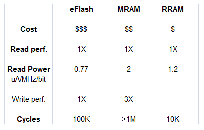
The catchiest quote of the day was with regards to the introduction of embedded Resistive-RAM (RRAM) and Magnetic-RAM (MRAM, based on spin-transfer torque technology):
“Emerging memory will finally emerge at 22nm.” 🙂
eRRAM
40nm eRRAM will be ready for production later this year. The qualification data indicates 10 yrs retention @85C, with 10K cycles.
eMRAM
22nm eMRAM will be available 12/18, with 10 years retention @150C, with >1M cycles.
Note that eMRAM is a random access technology. “Customers are working with us on the integration of eMRAM instead of SRAM arrays, in addition to replacing eFlash non-volatile embedded memory. We’re working on improving the natural yield of the eMRAM array.” (although I gathered that even with repair, an embedded MRAM architecture would include ECC)
MRAM qualification for the Automotive platform is underway — “We will provide a feasibility assessment on MRAM for Automotive in 2H’18.”
(2) advanced packaging technology
Another TSMC goal is to evolve their packaging technology — as Dr. Doug Yu, VP of Packaging Development said, “TSMC wants to be known as a system integration foundry.”
As a result, there are aggressive development plans for existing die-to-substrate bump attach technology for conventional packaging. And, significant R&D investment is being applied to a variety of new packaging options leveraging the existing CoWoS and InFO WLP technologies. “We intend to leverage our wafer-processing expertise in the development of advanced package technologies.”
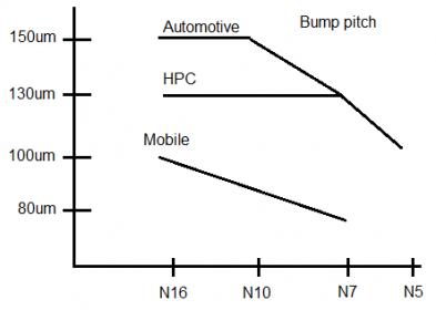
- Chip-on-Wafer-on-Substrate (CoWoS): larger interposer, finer Cu bump pitch, RDL L/S 0.4um/0.4um, 130um bump by YE18.
[INDENT=2]The key CoWoS development would be to support larger (composite) interposer designs, with a 2X max reticle size interposer available in early 2019.
- InFO-MS: 2um/2um RDL L/S, YE’18
[INDENT=2]The goal of the InFO-MS package offering is to integrate an SoC die with an HBM memory configuration, in an InFO footprint. SI/PI analysis flow requirements are extremely demanding (~1700+ nets). Full flow support for package layout, TSV design rules, and inter-die LVS is available. This packaging option should be qualified in 1H’19.
- InFO-AiP: integrate dipole and patch antennas in the package
[INDENT=2]
The antenna metal is integrated into the package — e.g., on the top surface separated from the RF chip by a dielectric layer, with through vias.
- InFO-on-Substrate: effectively, a 3D Systems-in-Package (SiP) stacking technology with an InFO-based module
(2) Reliability emphasis
A pervasive theme throughout the symposium was the investment in automotive grade qualification.
In that regard, a comment that stuck out was made by Dr. Cheng-Min Lin, Director of Automotive Business Development, “Time-Dependent Dielectric Breakdown (TDDB) is most critical failure mechanism for automotive applications. The traditional TDDB spec of ‘1 ppm after 3 years’ is now scaled to an aggressively low failure rate after 10 years. We are putting in place new quality screening methods, such as a ‘maverick lot quarantine’ policy, based on statistical wafer yield limits.”
This emphasis on product lifetime implies that designers will indeed need to apply additional focus on simulation with device aging and device breakdown mechanisms. The results of the new aging flow will emerge as a critical tapeout requirement.
And, consistent with the discussion on device reliability, the number one takeaway from the symposium also related to quality…
(1) “Quality Excellence”
J.K. Wang, VP of Fab Operations presented some amazing statistics. The process variants for the four platforms require tremendous coordination:
- 50K+ process module “recipes”
- 20M+ equipment tool settings
- 100K+ statistical process control (SPC) charts
- 10M+ fault detection and classification (FDC) charts (detect changing equipment conditions, incorporated into “preventive maintenance” policies)
TSMC has employed internal data management methods to review these millions of control charts, as part of a focus on reducing DPPM. Special attention is being applied to root cause analysis of “outlier” conditions. For example, a concerted effort was made to evaluate wafer edge data, to determine how yield could be improved in the outermost “zone” — a big financial benefit to high volume customers, for sure. For the automotive market, there is a major quality improvement initiative, including proposals such as “ink out good die in a bad zone”.
Also, TSMC is encouraging customers to collaborate with them on failure analysis of burn-in parts as part of their quality initiative – i.e., the “infant failures” of the bathtub curve. “We don’t want to wait for system test or field return failures to improve our focus on process control and improvement.”
To be sure, there were a lot of symposium presentations on advanced process node development, but I think this one really stood out as indicative of the customer partnerships and collaboration that TSMC continues to emphasize.
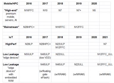
PS. To assist with the process node interpretation, here’s a summary that was presented for the Mobile (“premium” and “mainstream”), HPC, and IoT platforms.
-chipguy
Also Read:
Top 10 Updates from the 2017 TSMC Technology Symposium, Part I
Top 10 Updates from the 2017 TSMC Technology Symposium, Part II
Share this post via:


Comments
9 Replies to “Top 10 Highlights of the TSMC 2018 Technology Symposium”
You must register or log in to view/post comments.