Recently, TSMC held their annual Technology Symposium, providing an update on the silicon process technology and packaging roadmap. This article will review the highlights of the silicon process developments and future release plans.
Subsequent articles will describe the packaging offerings and delve into technology development and qualification specifically for the automotive sector. Several years ago, TSMC defined four “platforms” which would receive unique R&D investments to optimize specific technical offerings: high performance computing (HPC); mobile; edge/IoT computing (ultra-low power/leakage); and, automotive. The focus on process development for the automotive market was a prevalent theme at the Symposium, and will be covered in a separate article.
Parenthetically, these platforms remain the foundation of TSMC’s roadmap. Yet, the mobile segment has evolved beyond (4G) smartphones to encompass a broader set of applications. The emergence of the “digital data transformation” has led to increased demand for wireless communication options between edge devices and cloud/data center resources – e.g., WiFi6/6E, 5G/6G (industrial and metropolitan) networks. As a result, TSMC is emphasizing their investment in RF process technology development, to address this expanding segment.
General
Here are some general highlights from the Symposium, followed by specific process technology announcements.
- breadth of offerings
In 2020, TSMC extended their support to encompass 281 distinct process technologies, shipping 11,617 products to 510 customers. As in previous years, TSMC proudly stated “we have never shut down a fab.”
- capacity
Current capacity in 2020 exceeds 12M (12” equivalent) wafers, with expansion investments for both advanced (digital) and specialty process nodes.
- capital equipment investment
TSMC plans to invest a total of US$100 billion over the next three years, including a US$30 billion capital expenditure this year, to support global customer needs.
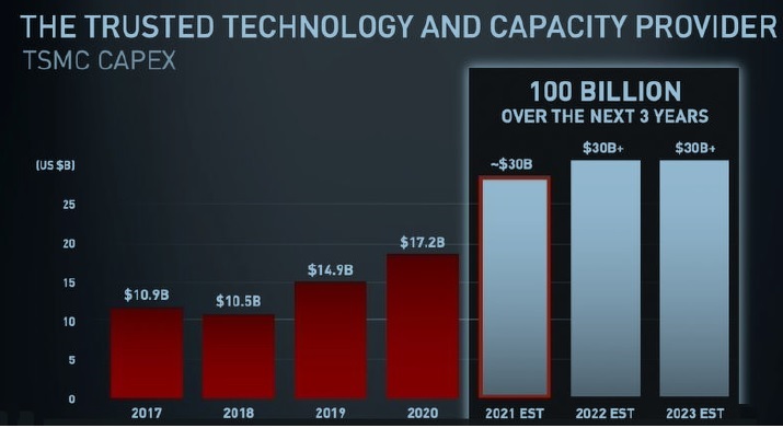
TSMC’s global 2020 revenue was $47.78B – the $30B annual commit to fab expansion certainly would suggest an expectation of significant and extended semiconductor market growth, especially for the 7nm and 5nm process families. For example, new tapeouts (NTOs) for the 7nm family will be up 60% in 2021.
- US fab
TSMC has begun construction of a US fab in Phoenix, AZ – volume production of the N5 process will commence in 2024 (~20K wafers per month).
- environmental initiatives
Fabs are demanding consumers of electricity, water, and (reactive) chemicals. TSMC is focused on transitioning to 100% renewable energy sources by 2050 (25% by 2030). Additionally, TSMC is investing in “zero waste” recycling and purification systems, returning used chemicals to “electronic grade” quality.
One cautionary note… Our industry is famously cyclic, with amplified economic upticks and downturns. The clear message from TSMC at the Symposium is that the accelerating adoption of semiconductors across all platforms — from data-intensive computation centers to wireless/mobile communications to automotive systems to low-power devices – will continue for the foreseeable future.
Process Technology Roadmap
- N7/N7+/N6/N5/N4/N3
The figure below summarizes the advanced technology roadmap.
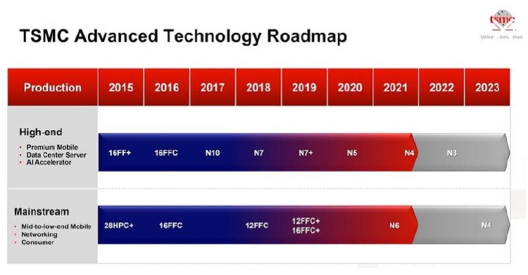
N7+ represents the introduction of EUV lithography to the baseline N7 process. N5 has been in volume production since 2020.
N3 will remain a FinFET-based technology offering, with volume production starting in 2H2022. Compared to N5, N3 will provide:
- +10-15% performance (iso-power)
- -25-30% power (iso-performance)
- +70% logic density
- +20% SRAM density
- +10% analog density
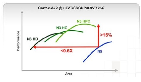
TSMC foundation IP has commonly offered two standard cell libraries (of different track heights) to address the unique performance and logic density of the HPC and mobile segments. For N3, the need for “full coverage” of the performance/power (and supply voltage domain) range has led to the introduction of a third standard cell library, as depicted below.
Design enablement for N3 is progressing toward v1.0 PDK status next quarter, with a broad set of IP qualified by 2Q/3Q 2022.
N4 is a unique “push” to the existing N5 production process. An optical shrink is directly available, compatible with existing N5 designs. Additionally, for new designs (or existing designs interested in pursuing a physical re-implementation), there are some available enhancements to current N5 design rules and an update to the standard cell libraries.
Similarly, N6 is an update to the 7nm family, with increasing adoption of EUV lithography (over N7+). TSMC indicated, “N7 remains a key offering for the increasing number of 5G mobile and AI accelerator designs in 2021.”
- N7HPC and N5HPC
An indication of the demanding performance requirements of the HPC platform is the customer interest in applying supply voltage “overdrive”, above the nominal process VDD limit. TSMC will be offering unique “N7HPC” (4Q21) and “N5HPC” (2Q22) process variants supporting overdrive, as illustrated below.
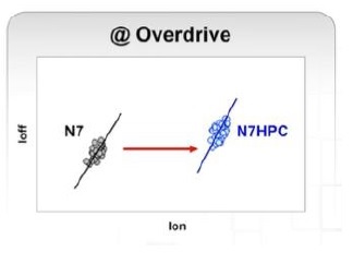
There will be a corresponding SRAM IP design release for these HPC technologies. As expected, designers interested in this (single digit percentage improvement) performance option will need to address increased static leakage, BEOL reliability acceleration factors, and device aging failure mechanisms. TSMC’s investment in the development and qualification of processes specifically optimized for individual platforms is noteworthy. (The last HPC-specific process variant was at the 28nm node.)
- RF technology
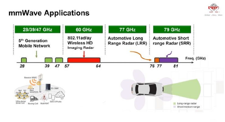
The market demand for WiFi6/6E and 5G (sub-6GHz and mmWave) wireless communications has led TSMC to increase focus on process optimizations for RF devices. RF switches are also a key application area. Low power wireless communication protocols, such as Bluetooth (with significant digital integration functionality) are a focus, as well. Automotive radar imaging systems will no doubt experience growing demand. The mmWave applications are summarized in the figure below.
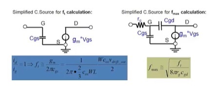
The two key parameters typically used to describe RF technology performance are:
- device Ft (“cutoff frequency”), where current gain = 1, inversely proportional to device channel length, L
- device Fmax (“maximum oscillation frequency”), where power gain = 1, proportional to the square root of Ft, inversely proportional to the square root of Cgd and Rg
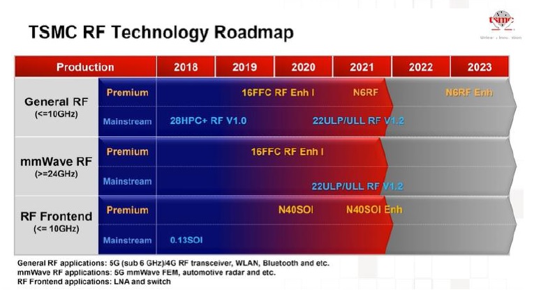
The TSMC RF technology roadmap is shown below, divided into different application segments.
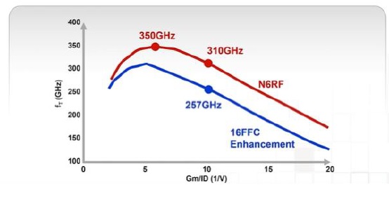
- N6RF
The N6RF process was highlighted at the Symposium – a device performance comparison to N16FFC-RF is shown below.
The N28HPC+RF and N16FFC-RC processes also recently received enhancements – for example, improvements in the parasitic gate resistance, Rg, were highlighted. For low-noise amplifier (LNA) applications, TSMC is evolving their SOI offerings at 130nm and 40nm.
- ULP/ULL Technologies
IoT and edge device applications are forecast to become more pervasive, demanding increasing computational throughput at very low power dissipation (ULP) combined with ultra-low leakage (ULL) static power dissipation for improved battery life.
TSMC has provided ULP process variants – i.e., operational functionality for IP at very low VDD supply voltage. TSMC has also enabled ULL solutions, with devices/IP utilizing optimized threshold voltages.
An overview of the IoT (ULP/ULL) platform and process roadmap is given below.
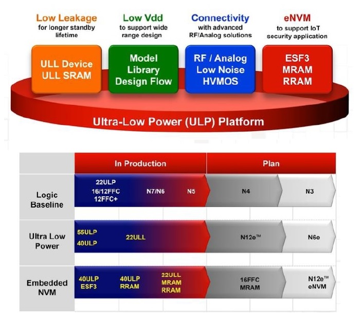
The N12e process node was highlighted by TSMC, integrating an embedded non-volatile memory technology (MRAM or RRAM), with standard cell functionality down to 0.55V (using SVT devices; low Vt cells would enable lower VDD and active power at higher leakage). Comparable focus has been made to reduce the Vmin and standby leakage current of N12e SRAM IP, as well.
Summary
At the Symposium, TSMC introduced several new process developments, with specific optimizations for HPC, IoT, and automotive platforms. RF technology enhancements are also a focus, in support of rapid adoption of new wireless communications standards. And, to be sure, although it didn’t receive much emphasis at the Symposium, there is a clear execution roadmap for the advanced mainstream process nodes – N7+, N5, and N3 – with additional continuing process improvements as reflected in the release of intermediate nodes N6 and N4.
For more information on TSMC’s digital technology roadmap, please follow this link.
-chipguy
Share this post via:


Comments
There are no comments yet.
You must register or log in to view/post comments.