Recently, TSMC held their 26th annual Technology Symposium, which was conducted virtually for the first time. This article is the first of three that attempts to summarize the highlights of the presentations.
This article focuses on the TSMC process technology roadmap, as described by the following executives:
- Y.J. Mii, SVP, R&D: “Advanced Technology Leadership”
- Kevin Zhang, SVP, Business Development: “Specialty Technology Leadership”
- Y.P. Chin, SVP, Operations: “Manufacturing Excellence”
Key Takeaways
- The N7 to N5 to N3 process node cadence continues on an aggressive schedule, with each transition offering a full-node areal scaling.
- N3 will utilize a traditional FinFET device architecture.
- The new node N12e introduces an ultra-low power offering – the cell library VDD is reduced to 0.4V.
- The availability of alternative non-volatile memory technologies (RRAM, MRAM) offers continued scaling of applications requiring embedded NVM memory (eFlash). The availability of (high-endurance, SRAM-like) MRAM provides very interesting memory cache system design opportunities.
- TSMC is planning a huge R&D investment for technology development past N3.
N7, N5, and N3 Roadmap
N7 entered high volume manufacturing (HVM) in 2018, at Fab 15. TSMC provided a forecast for more than 200 N7/N7+ new tapeouts (NTOs) in 2020.
Recall that the initial N7 process definition did not incorporate EUV lithography – the subsequent N7+ process added EUV as a replacement for a few critical-dimension layers. Node N6 will offer a logic density boost (~18%) over N7, using a block-level physical re-implementation flow with a new Foundation IP library – e.g., mask layer reduction, CPODE cell abutment.
The next node, N5, entered HVM in 2Q2020, at Fab 18 in Tainan. EUV lithography has been applied extensively. (Fab 18 broke ground in January, 2018, with equipment move-in a year later – this is an extremely impressive ramp from fab construction to HVM, especially with EUV litho.)
A future N5+ variant will provide a ~5% performance boost, with HVM in 2021. Node N4 is a mid-life kicker to N5, with a mask layer cost reduction (while maintaining design rule capability to existing N5 IP). Risk production for N4 is 4Q21, with HVM in 2022.
N3 is well-defined, with EDA vendors already providing design enablement flows and with IP in active development – risk production is planned for 2021, with HVM in 2H22.
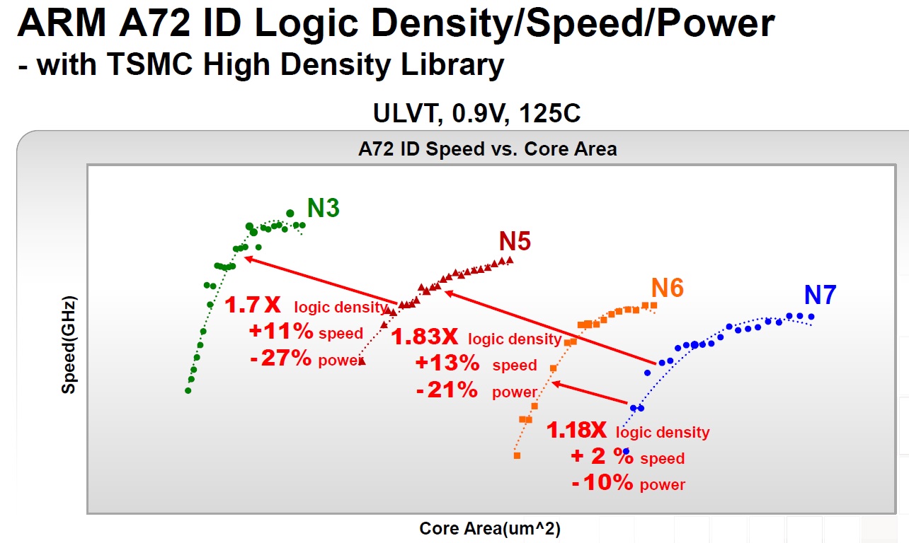
TSMC provided two charts to illustrate the PPA comparisons between these nodes. The first depicts the comparisons for an Arm A72 core. Recall that TSMC has focused their Foundation IP development and EDA enablement for different platforms – the comparison below utilizes the high-density based physical implementation flow associated with the Mobile and IoT platforms.
The high-performance platform (HPC) comparison for N7, N5, and N3 is shown below, using the physical implementation of the Arm A78 core as the reference.
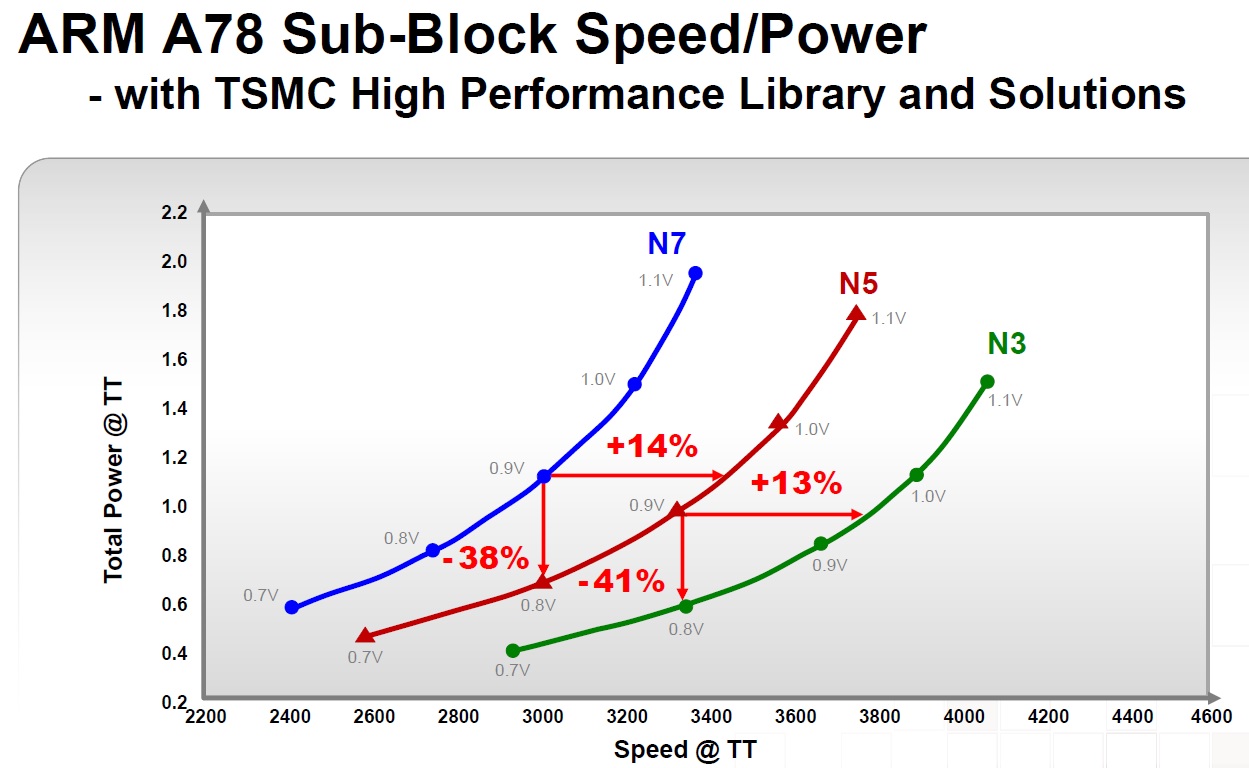
The way to interpret these curves is that a horizontal line represents the performance gain at iso-power, which the vertical line depicts the power gains at iso-performance.
In both cases, the N7 to N5 and N5 to N3 transitions incorporate a full-node areal density increase, although it should be noted that the SRAM IP and analog density scaling factors are less.

N12e
The IoT and mobile platforms are driven by the need for ultra-low power dissipation, achieved through supply voltage reduction and the availability of ultra-low leakage (ULL, high Vt) devices. Additionally, an ultra-low leakage SRAM bit cell offering is needed. Also, a new class of applications – AIoT, or Artificial Intelligence of Things – is emerging for the edge-centric, ultra-low power market.
TSMC introduced a new process designation, N12e, specifically to address these requirements – working from the N12FFC+ baseline, N12e is currently in risk production status. The N12e offering includes several key characteristics:
- cell library IP operating at VDD = 0.4V
- significant focus on statistical process control, to minimize device variation
- 0.5X power (@ iso-performance) compared to N22ULL
- 1.5X performance (@ iso-power) compared to N22ULL
The application of VDD=0.4V necessitates focus on the EDA flows for delay calculation/static timing analysis and coupled noise electrical analysis – the status of the EDA enablement for N12e will be covered in a subsequent article. (Please refer to: http://n12e.tsmc.com.)
RF Roadmap
To support the rapidly growing 5G market, TSMC has maintained focus on RF CMOS process development, striving for enhanced device characteristics. The current RF offerings are based on the N28HPC and N16FFC processes.
The new RF roadmap introduced N6RF, with significantly improved power and device noise factor (NF, @5.8GHz) over current devices. Design kit enablement for N6RF will be released in 2Q21.
Non-volatile memory (NVM) Roadmap – eFlash, RRAM, and MRAM
TSMC’s current embedded flash memory IP for the N28HPC (HKMG) node is being qualified for the automotive design platform (i.e., endurance cycles and data retention at 150C) – target date is end of 2020.
For process nodes after N28, scaling of floating gate-based flash memory becomes more difficult (expensive). The NVM roadmap transitions to Resistive (filamentary) RAM, with N22 tapeouts this year (at 125C, non-automotive grade). Magneto-resistive RAM (MRAM) is also available for N22 tapeouts, with automotive grade qualification in 4Q20. Further, N16 MRAM IP will be available for risk production in 4Q21.
Initially, RRAM and MRAM technologies will be used as IP replacing eFlash applications – e.g., 10K+ endurance cycles. TSMC indicated an “SRAM-like” MRAM IP offering for N16 will be available in 4Q22 – clearly, significant focus is being applied to increase MRAM endurance. MRAM as a non-volatile, high-density L3/L4 SRAM-replacement memory cache will offer some very unique system architecture design opportunities.
Advanced process node fab capacity
To support the demand for nodes N16 to N5, 300mm wafer Gigafab capacity has experienced a CAGR of 28% from 2016 to 2020. The fab capacity for N7 alone has grown 3.5X in just over two years, from 2018 to 2020. Additionally, the capacity for N5 is planned for 3X growth from today to 2022.
Y.P. Chin highlighted that EUV learning from N7+ and N5 has enabled an extremely aggressive improvement in defect density (D0). For example, refer to the innovation that TSMC has deployed for EUV mask cleaning: link.
There are also major expansion plans for the Advanced Packaging line facilities in Tainan.
R&D Investment
A consistent theme through the presentations was the extensive investment TSMC is making in future technology R&D. Specifically, TSMC is building a new R&D Center in Hsinchu, as depicted below. The goal will be to enable “thousands of engineers” to work on new transistor architectures, materials, and process flows required for the nodes after N3, and “for the next twenty years” – more on these initiatives shortly.
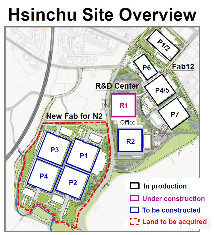
Construction of the R&D center got underway in 1Q20, with occupancy starting in 2021.
Adjacent to the new R&D center, TSMC illustrated new fab construction in Hsinchu specifically designated for the “N2” process node. Like the other TSMC Gigafabs – e.g., Fab 12, Fab 15, Fab 18, — the N2 fab construction will evolve in multiple phases.
The planned investment in R&D and fab deployment for “N2 and beyond” is definitely impressive.
Future Technology R&D
TSMC provided a glimpse into some of the future technologies currently being investigated, as the R&D activity continues to ramp.
- RC enhancements
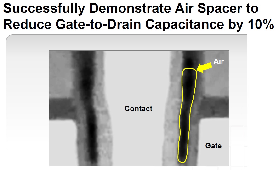
FinFET devices offer significant benefits in areal drive current and subthreshold leakage electrostatic channel control over planar devices – yet, one of the disadvantages is the additional Cgs and Cgd parasitic capacitance from the gate traversal over the fin(s) and the raised source/drain plus M0 metallization. TSMC will be introducing an air-gap process in the dielectric between gate and source/drain to reduce these parasitics.
Additionally, interconnect R*C delays will be improved with the introduction of a new via trench barrier process.
- EUV litho development
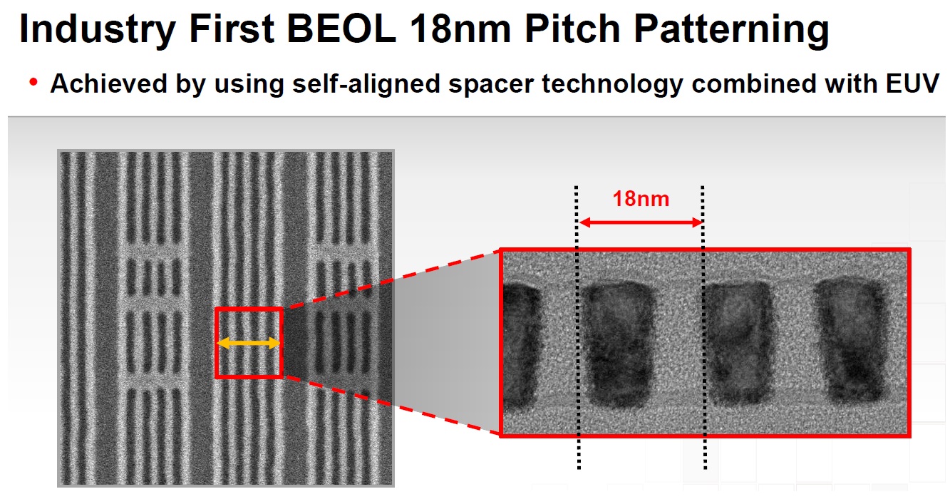
To enable aggressive lithography scaling for pitches less than 80nm using 193i illumination, TSMC introduced mask data decomposition (“coloring”) at the N20 node. Double and quad multipatterning (SADP or 2P2E, and SAQP) have enabled further scaling. Inverse lithography technology (ILT) algorithms, as part of a source-mask optimization (SMO) mask data preparation methodology, was also deployed. 13.5nm EUV lithography was introduced for N7+, as mentioned above. To enable further scaling, EUV multipatterning (2P2E) is required.
TSMC showed lithographic patterning/etch in support of an 18nm interconnect pitch.
- high NA EUV
The numerical aperture of a lithography system defines the resolution capability, a function of the cone of light captured and the refractive index of the entire lens system. The resolution is inversely proportional to the NA. TSMC is working closely with ASML on the next generation of “high NA” EUV equipment and corresponding resist technology, to enable finer resolution in future nodes.
- GAA nanosheets
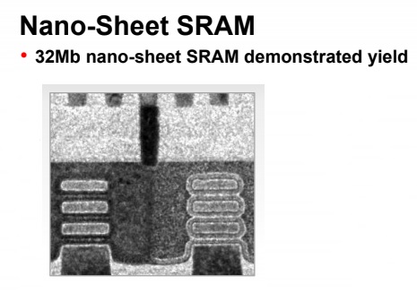
TSMC highlighted their R&D efforts to implement gate all-around nanosheets, as a FinFET replacement.
The N3 process definition starts with a conventional FinFET device. (To achieve increased performance and fin pitch, the fin height and aspect ratio for N3 will need to be improved.)
As has been the case for TSMC node transitions, adhering to the roadmap schedule has been a paramount priority. Y.J. Mii said, “After carefully evaluating customer needs and technology maturity, N3 continues to use FinFET devices. Our R&D team has extensive experience with nanowire and nanosheet technology, and have demonstrated 32Mb SRAM testsite yield. We will have the technology options for each new node ready in advance – the right technology at the right time.” It will be interesting to see how GAA device architectures evolve.
- unique “2D” device semiconducting channel material
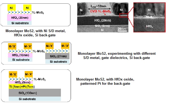
TSMC referred to a technical paper published earlier this year, showing promising results for a replacement to the Si (or SiGe) FinFET device. Semiconducting “monolayers” of MoS2 serve as the (planar) field-effect device channel, offering improved carrier mobility. (Reference: A.S. Chou, et al., VLSI Symposium 2020).
The figure below illustrates a single monolayer of MoS2, the HfO2 gate dielectric, and either a (large area) Si or a local Pt “back gate” device structure. The device drive current and Ion/Ioff ratio shows great promise – reducing the contact resistance (Rc) from the S/D metal to the semiconducting layer is a key process development challenge.
- carbon nanotubes
TSMC also referred to a recently published paper illustrating the implementation of a deposited layer of carbon nanotubes (CNT) for a unique application. The nanotubes were incorporated as part of the (low temperature-restricted) back-end-of-line flow in N28, with patterning of gate and source/drain metallization. The specific application for which these devices are targeted is for the logic circuit power-gating “header”. (Reference: Cheng, et al, IEDM, 2019, paper 19.2)

Current power-gating implementations utilize multiple silicon devices (low R) connected between the “always on” and switched power rails connected to the block logic. These designs require unique block-level physical design, specific cell library images, and modified (global/local) power distribution networks, adversely impacting areal circuit density and routability. A semiconducting CNT power gating circuit could offer a significant PPA boost – ongoing focus on reducing the overall series “on” resistance will be key.
As an aside, it is perhaps unwise to read too much into the R&D part of the Symposium presentations, in terms of what was and was not mentioned for post-N3 architectures. Nevertheless, the following options being widely investigated within the semiconductor industry were not discussed: negative-capacitance FETs (NC-FETs, integrating ferroelectric materials), vertical nanowires (VNW), tunnel FETs, or N3XT (“full 3D” die integration of logic, memory, and NVM).
Look for subsequent articles highlighting TSMC packaging technology and design enablement presentations to follow.
-chipguy
Highlights of the TSMC Technology Symposium – Part 2
Highlights of the TSMC Technology Symposium – Part 3
Share this post via:


Comments
5 Replies to “Highlights of the TSMC Technology Symposium – Part 1”
You must register or log in to view/post comments.