Using Soft IP and Not Getting Burned

Using Soft IP and Not Getting Burned
by Daniel Payne on 02-07-2013 at 10:11 am

The most exciting EDA + Semi IP company that I ever worked at was Silicon Compilers in the 1980’s because it allowed you to start with a concept then implement to physical layout using a library of parameterized IP, the big problem was verifying that all of the IP combinations were in fact correct. Speed forward to today and our industry still faces the same dilemas, how do you assemble a new SoC designed with hard and soft IP, and know that it will be functionally and physically correct?

They say that it takes a village to raise a child, so then in our SoC world it takes collaboration between Foundry, IP providers and EDA vendors to raise a product. One such collaboration is between:

These three companies are hosting a webinar on Tuesday, March 5, 2013 at 9AM, Pacific time to openly discuss how they work together to ensure that you can design SoCs with Soft IP and not get burned.

Agenda

  • Moderator opening remarks
    Daniel Nenni (SemiWiki) (5 min)

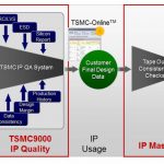
  • The TSMC Soft IP Alliance Program – structure, goals and results
    (Dan Kochpatcharin, TSMC) (10 min)

  • Implementing the program with the Atrenta IP Kit
    (Mike Gianfagna, Atrenta) (10 min)

  • Practical results of program participation
    (John Bainbridge, Sonics) (10 min)

  • Questions from the audience (10 min)

Speakers

Daniel Nenni
Founder, SemiWiki
Daniel has worked in Silicon Valley for the past 28 years with computer manufacturers, electronic design automation software, and semiconductor intellectual property companies. Currently Daniel is a Strategic Foundry Relationship Expert for companies wishing to partner with TSMC, UMC, SMIC, Global Foundries, and their top customers. Daniel’s latest passion is the Semiconductor Wiki Project (www.SemiWiki.com).


John Bainbridge
Staff Technologist, CTO office, Sonics, Inc.
John joined Sonics in 2010, working on System IP, leveraging his expertise in the efficient implementation of system architecture. Prior to that John spent 7 years as a founder and the Chief Technology Officer at Silistix commercializing NoC architectures based upon a breakthrough synthesis technology that generated self-timed on-chip interconnect networks. Prior to founding Silistix, John was a research fellow in the Department of Computer Science at the University of Manchester, UK where he received his PhD in 2000 for work on Asynchronous System-on-Chip Interconnect.


Mike Gianfagna
Vice President, Corporate Marketing, Atrenta
Mike Gianfagna’s career spans 3 decades in semiconductor and EDA. Most recently, Mike was vice president of Design Business at Brion Technologies, an ASML company. Prior to that, he was president and CEO for Aprio Technologies, a venture funded design for manufacturability company. Prior to Aprio, Mike was vice president of marketing for eSilicon Corporation, a leading custom chip provider. Mike has also held senior executive positions at Cadence Design Systems and Zycad Corporation. His career began at RCA Solid State, where he was part of the team that launched the company’s ASIC business in the early 1980’s. He has also held senior management positions at General Electric and Harris Semiconductor (now Intersil). Mike holds a BS/EE from New York University and an MS/EE from Rutgers University.


Dan Kochpatcharin
Deputy Director IP Portfolio Marketing, TSMC
Dan is responsible for overall IP marketing as well as managing the company IP Alliance partner program.
Prior to joining TSMC, Dan spent more than 10 years at Chartered Semiconductor where he held a number of management positions including Director of Platform Alliance, Director of eBusiness, Director of Design Services, and Director of Americas Marketing. He has also worked at Aspec Technology and LSI Logic, where he managed various engineering functions.

Dan holds a Bachelor of Science degree in electrical engineering from UC Santa Barbara, a Master of Science in computer engineering, and an MBA from Santa Clara University.

Registration
Sign up here.


Wall Street Does NOT Know Semiconductors!

Wall Street Does NOT Know Semiconductors!
by Daniel Nenni on 01-20-2013 at 6:00 pm

In my never ending quest to promote the fabless semiconductor ecosystem I cannot pass up a discouraging word about one of the oldest financial services companies. You can consult with me for $300 per hour to answer your questions about the semiconductor industry on the phone or you can buy me lunch and get it in person (lunch will probably cost you more). The people who hire me are usually financial types (hedge fund managers etc…) but I also get called by semiconductor companies for market strategies and such. SoCs are a popular topic now and things get busy when quarterly results come in for TSMC, Intel, and the fabless guys in the mobile market segment. The fun part is taking apart analyst reports like the recent one from Morgan Stanley about TSMC.

Since its founding in 1935, Morgan Stanley and its people have helped redefine the meaning of financial services. The firm has continually broken new ground in advising our clients on strategic transactions, in pioneering the global expansion of finance and capital markets, and in providing new opportunities for individual and institutional investors. Click below to see a timeline of Morgan Stanley’s growth, which parallels the history of modern finance.

To start, look at the Morgan Stanley Wikipedia page which lists controversies and lawsuits with fines in the hundreds of millions of dollars.

TSMC released Q4 2012 numbers during last week’s conference call. You can read the Seeking Alpha transcript HERE. I’m a big fan of the Seeking Alpha transcripts, reading is much better than listening, unfortunately the Seeking Alpha analysts don’t know semiconductor either but more on that later.

Per Morgan Stanley:

[LIST=1]

  • 28nm is surprising on the upside (DUH)
  • 28nm Margins above expectations (DUH)
  • 20nm node to be bigger than 28nm (WRONG)
  • TSMC 6.5% Q1 revenue drop (WRONG)

    Disclaimer: This information came from a phone call so it may not be 100% accurate but it has been repeated by other analysts so they are valid discussion points.

    Morgan Stanley and others were surprised at the TSMC Q4 financial numbers which they should not have been. As I blogged before, 28nm will be the most successful node we have seen in a long time (in all regards) and TSMC owns it, thus the high margins. To be fair, TSMC warned that Q4 could be soft but I blogged otherwise. TSMC is a conservative company and can certainly play the Wall Street game. On the other hand, I would rather see ACCURATE forecasts from analysts so we can do business without shortages, layoffs, and the other things that go along with bad business decisions.

    In what way will 20nm be bigger than 28nm? Compare the value proposition of 28nm and 40nm versus 20nm and 28nm in regards to price, performance, and power consumption. The value proposition of 20nm is less than half of 28nm meaning some companies will do limited tape-outs at 20nm, some are even skipping 20nm completely in favor of 14nm FinFETs which should ramp shortly after 20nm. Samsung, GLOBALFOUNDRIES, and TSMC will all use Gate-Last HKMG and have 20nm production simultaneously so heated competition will be a factor. TSMC has the advantage of being on their second generation of the Gate-Last HKMG experience since Samsung and GLOBALFOUNDRIES used Gate-First at 28nm which did not yield as well. Samsung has the “Brute Force” 20nm advantage with what seems like unlimited resources and fab capacity. Samsung is also an IDM with internal SoC/VLSI design experience. GLOBALFOUNDRIES has the advantage of being the designated second source foundry by companies like Qualcomm and other big fabless companies that see Samsung as a ruthless competitor. The GLOBAFOUNDRIES New York fab is 20nm so customers can keep their IP protected under American law.

    Bottom line: 20nm is a completely different game than 28nm so any comparison will be much more complicated, be very careful who you listen to, my opinion.

    Q1 will be like Q4, underestimated, but that is all part of the Wall Street game. There is no stopping the mobile market, 28nm owns mobile, TSMC owns 28nm, simple as that. Seeking Alpha is still perpetuating the Apple at TSMC 28nm misinformation and, in general, I’m not impressed at all with their semiconductor coverage. If you read them do a quick author look up on LinkedIn. If they don’t have a profile there is probably a good reason for it. If they do, look for at least some semiconductor experience before investing your hard earned money their way.

    Also read: TSMC Apple Rumors Debunked!


  • Mentor @ the TSMC Open Innovation Platform Forum

    Mentor @ the TSMC Open Innovation Platform Forum
    by glforte on 01-16-2013 at 6:16 pm

    At TSMC’s Open Innovation Platform (OIP) Ecosystem Forum, Mentor made technical presentations on four different topics, two of them co-presented with TSMC and LSI Corporation. Those presentations are described below with links to downloadable pdf presentation files.

    Finding and Fixing Double Patterning Errors in 20nm Design

    David also won the Customer’s Choice award (selected by attendee vote) for his presentation on Finding and Fixing Double Patterning Errors in 20nm Designs at TSMC’s Open Innovation Platform ecosystem event. In this presentation, David describes the new constraints that double patterning brings to the 20nm node, and how IC designers can deal with DP related design rule violations. View presentation…

    A Platform for TSMC’s CoWoS 3DIC Reference Flow

    The first phase of 3DIC adoption will be based on silicon interposers. Designing multi-die systems using this technology introduces new challenges for the EDA design flow. At the TSMC OIP event, Mentor described solutions for 3DIC design specifically tailored to TSMC manufacturing processes.View presentation

    Automated Approach for Waiving Physical Verification Errors in IP

    Redundantly reviewing recurring errors during custom and third-party IP integration can slow down SoC verification. An automated waiver management methodology enables design and verification teams to specify and process a variety of design rule waivers, reducing debugging time and improving SoC results. Mentor and LSI recently described the use of this technology at the TSMC OIP event. View presentation

    Improving IC Design for Reliability

    Verification of 20nm designs is expected to bring significant challenges. A robust verification methodology that addresses circuit reliability is increasingly difficult. At 20nm, new devices that incorporate thin oxides are less robust and more subject to electrical overstress (EOS) failures. The increased use of mixed-signal and multi-voltage design techniques also increases the likelihood that transistors could be implemented in an incorrect voltage domain. At TSMC’s recent OIP event, Mentor showed techniques to prevent long term electrical failure using new tools to validate ESD structures, protect against EOS, manage multiple power domains, and carefully balance sensitive analog circuits. View presentation


    TSMC Apple Rumors Debunked!

    TSMC Apple Rumors Debunked!
    by Daniel Nenni on 01-11-2013 at 8:00 am

    Disclaimer: I’m a blogger and by definition I share my observations, opinions, and experiences. Journalists and Analysts on the other hand are held to a much higher legal standard which is why they cite undisclosed sources and use double speak to shield themselves legally. Why trust a SemiWiki blogger over a Journalist or an Analyst? Because we actually work inside the fabless semiconductor ecosystem and they do not, simple as that. My previous TSMC blogs are HERE if you want to check my credentials. Be sure and read the ones early last year on the rumors of problems with TSMC 28nm. I said FALSE and I was right, the Journalists and Analysts were wrong, and their pants are on fire once again.

    The first rumor is that the next Apple A7 processor (28nm) will be made by TSMC. That rumor is FALSE! As I previously blogged, the Apple iPhone to be released this year (iPhone 5s) will be Samsung 28nm. The iPhone to be released next year (iPhone 6) will be TSMC 20nm. A company the size of Apple cannot switch foundries on a moment’s notice. The volumes are too high and the technology issues are too complex.I have no doubt Apple discussed 28nm with TSMC but since no other foundries had 28nm available there was no way TSMC could handle the wafer demands of Apple and the rest of the fabless companies. Apple also gets preferred pricing so why would TSMC give up higher margin 28nm business AND alienate their customer base? Not going to happen.

    TSMC: Our mission is to be the trustedtechnology and capacity provider of the global logic IC industry for years to come.

    20nm will be another story. Samsung and GLOBALFOUDNRIES will have 20nm in production and TSMC will see their 28nm customers use other sources. Qualcomm, TI, Broadcom, Marvell, and Xilinx all second and third source wafer manufacturing when possible. 20nm volumes will also not match 28nm due to a higher cost per transistor. To me 20nm is a half node in the economic sense in preparation for 16/14nm FinFETs, which will hit much higher volumes from the mobile guys due to lower power consumption (longer battery life).

    The second rumor is that TSMC will build a fab in New York to help facilitate Apple business. I say FALSE. If TSMC builds a GigaFab anywhere in the United States I will eat my SemiWiki hat, simple as that.If TSMC needs to expand capacity above and beyond what they have planned today they can simply take over empty DRAM fab space in Taiwan which there is plenty of. Or if you want a more realistic rumor to spread here it is: TSMC will acquire the #3 semiconductor foundry UMC to increase capacity. This is much better than the rumor last year that GLOBALFOUNDRIES would acquire UMC. But I don’t do rumors so you didn’t hear it from me.

    The Taiwan government founded the pure-play semiconductor foundry business working hand-in-hand with both TSMC and UMC. TSMC and UMC are brothers. The Taiwan economy is semiconductor centric. TSMC is one of Taiwan’s top employers. I have no doubt that TSMC is seriously looking at all options but why would they follow the GLOBALFOUNDRIES model of having “global foundries” in favor of the TSMC model of Taiwan based cost efficiencies? The U.S. environmental impact bureaucracy alone would kill that deal! :p The wafer business has always been about price and that will never change.The other prediction I made last year is that TSMC stock (TSM) is a $20 dollar stock. It will happen this year, believe it.That’s my story and I’m sticking to it.

    Related: Apple will NOT manufacture SoCs at Intel!


    Wafer Costs: Out of Control or Not?

    Wafer Costs: Out of Control or Not?
    by Paul McLellan on 01-01-2013 at 8:30 pm

    I didn’t attend the International Electronic Device Meeting (IEDM) earlier this month, but there have been a lot of reports on the inter webs especially about 20nm and 14nm processes. Some of this is really geeky stuff but I think that perhaps the most interesting thing I’ve read about is summarized in this chart:

    This shows the wafer costs (12″, 30cm wafers) for 28nm, 20nm and then 14nm with multiple patterning and, in purple, 14nm with EUV lithography. The chart comes from Luc van den Hove, chief executive of IMEC in Belgium.

    These are raw wafer costs and thus haven’t been adjusted for the increase in transistor (and perhaps interconnect) density. Typically when we transition from one process node to the next, the wafer costs go up a little bit but that is completely dominated by the increase in how much we can put on a given sized die, and so the cost per transistor drops substantially. This is the economic driver of Moore’s law and is what makes it possible to have a $500 iPhone deliver more computer power than a 1980s mainframe that cost millions of dollars.

    But these costs are going up dramatically. The Y-axis scale doesn’t start at zero so the picture is a bit misleading, 14nm costs are not three times 28nm. But they are nearly twice. If the process truly scaled everything then the density of transistors at 14nm would be four times that of 28nm so cost per transistor would still be falling fast. But increasingly the transistor length is only the headline number for the process and the interconnect is shrinking much more slowly, if at all. When you look at the pitches for various layers in a modern process it is impossible to see anything close to 2X the headline number.

    So the key question is whether 14nm will have an economic driver or just a technology driver for those few designs that can truly take advantage of the increased density and decreased power, even though there may even be a cost penalty. For Apple’s iPhone and Samsung’s Android phones probably. For those $50 smartphones for developing countries that won’t work.

    Despite the purple bar looking optimistic, the received wisdom is that EUV is now too late for 14nm and so we will have to have a lot of double and triple patterning instead (which is one of the things that drives the cost up so much). EUV works in the sense that you can flash some wafers but the current state-of-the-art seems to be about 20 wafers/hour versus the 100 or 200/hour that is required to make the approach viable. The intensity of the light source (droplets of tin zapped with a huge laser) is too low, the mirrors (which aren’t really mirrors in the usual sense) absorb too much of the light, and there are too many reflections required between the source and the photoresist. Not much energy makes it to the resist to make the exposure.

    On a more optimistic note, Intel claimed that their costs per transistor were falling with each process node. Apparently they also don’t use double patterning at 20nm and there are two reasons for this. Firstly, they can have as restrictive design rules as they like, since they are the ultimate IDM with a limited product range. Secondly, most of the pitches at 20nm are not much different from 28nm. As I said above, only the FinFET transistor is 20nm or 22nm long.

    Anyway, 2013 will be the year we find out what 20nm and 14nm really can deliver as these processes start to ramp up. As Yogi Berra said, “the future ain’t what it used to be.” (although you have to be careful with Yogi Berra quotes. As he also (maybe) said, “I didn’t say all the things I said.”)


    Intel 22nm SoC Process Exposed!

    Intel 22nm SoC Process Exposed!
    by Daniel Nenni on 12-27-2012 at 9:00 pm

    The biggest surprise embedded in the Intel 22nm SoC disclosure is that they still do NOT use Double Patterning which is a big fat hairy deal if you are serious about the SoC foundry business. The other NOT so surprising thing I noticed in reviewing the blogosphere response is that the industry term FinFET was dominant while the Intel invented term Tri-Gate was rarely used.

    The transistor pitch – essentially the distance between two transistors – in the 22nm tri-gate technology is 80nm, which is the smallest pitch that can be produced using single-pattern lithography, Bohr says. “The next generation, 14,” he said, “we’re going to have to convert to Double Patterning to get tighter pitches.”

    Mark Bohr is the infamous Intel Senior Fellow who mistakenly predicted the doom of the fabless semiconductor ecosystem. Mark is a funny guy. I remember him putting up an incomplete 22nm defect density trend slide at this year’s Intel Developers Forum and saying “Was it a mistake that I left the numbers out? Yes! Oh my goodness, how could I have done that? But, gee, time is up, so … ”

    TSMC on the other hand presents their process defect density numbers every year at the TSMC Tech Symposium. Transparency equals trust in the foundry business, believe it.Back to Double Patterning, I will defer to the experts at Mentor for a complete description. Please see the Double Patterning Exposed articles for technical detail. No registration is required, just click on over.

    So the question is: Why does TSMC use the extra lithography steps of Double Patterning for 20nm and Intel does not for 22nm? The answer is Restrictive Design Rules which essentially eliminates any variability in orientation of shapes on critical layers. Intel is very comfortable with incredibly restrictive design rules since they are a microprocessor manufacturer and not a pure-play foundry. Intel can micromanage every aspect of design and manufacturing down to the electron. TSMC on the other hand needs to accommodate different design requirements and intellectual property from 615 customers.In addition to more flexible metal routing, Double Patterning also enables a tighter metal pitch which will put TSMC 16nm head-to-head with Intel 14nm even though, as I explained in 16nm FinFET Versus 20nm Planar, 16nm FF leverages 20nm process technology.

    It will be interesting to see how Intel tackles the Double Patterning challenge without the support of the mighty fabless semiconductor ecosystem.Which brings me to another trending topic: Is 20nm Planar a full node, half node, or everybody gonna skip node?

    I can tell you as a matter of fact that the top semiconductor companies around the world will NOT skip 20nm. 20nm tape-outs are happening now with production silicon late next year. 20nm will require more processing time from GDS to wafer but it will NOT be cost prohibitive for high volume customers. You are probably familiar with the 80/20 rule where 80% of something or other is controlled by 20% of the people, in the semiconductor industry we call it the 90/10 rule where 90% of the of the silicon shipped is by 10% of the companies and you can bet that they will tape out at 20nm. Designing at 20nm planar will also make the transition to 16nm FinFET easier and I can tell you that EVERYONE will be taping out at 16nm FinFET. That’s my story and I’m sticking to it.

    My favorite Mark Bhor quote: “We don’t intend to be in the general-purpose foundry business, I don’t think the volumes ever will be huge for Intel”. Exactly! So what is Intel going to do with all that empty fab space?


    IP Scoring Using TSMC DFM Kits

    IP Scoring Using TSMC DFM Kits
    by Daniel Payne on 12-20-2012 at 11:00 am

    Design For Manufacturing (DFM) is the art and science of making an IC design yield better in order to receive a higher ROI. Ian Smith, an AE from Mentor in the Calibre group presented a pertinent webinar, IP Scoring Using TSMC DFM Kits. I’ll provide an overview of what I learned at this webinar. Continue reading “IP Scoring Using TSMC DFM Kits”


    Cortex-A9 speed limits and PPA optimization

    Cortex-A9 speed limits and PPA optimization
    by Don Dingee on 12-19-2012 at 3:01 pm

    We know by now that clock speeds aren’t everything when it comes to measuring the goodness of a processor. Performance has direct ties to pipeline and interconnect details, power factors into considerations of usability, and the unspoken terms of yield drive cost.

    My curiosity kicked in when I looked at the recent press release from Cadence announcing they had reached 2.2 GHz on a 28nm dual-core ARM Cortex-A9 with Open Silicon. Are we reaching the limits of the Cortex-A9 in terms of clock speed growth? Or are more improvements in power, performance, and area (PPA) in store for the core?

    The raw percentages quoted by Cadence in that release sound great: 10% reduction in design area, 33% reduction in clock tree power, 27% reduction in leakage power compared to an unnamed prior design flow. These new figures were achieved with a combination of the latest RTL compiler, RTL-to-GDSII core optimization, and clock concurrent optimization techniques, which are really targeted at 20nm design but are certainly applicable to less aggressive nodes.

    We may be pressing the limits on what the Cortex-A9 core can do at 28nm, and there is likely only one more major speed bump to 20nm in store for the Cortex-A9. I went hunting and found several data points.

    ST-Ericsson has (had?) a 2.3 GHz version, with rumbles of 2.5 GHz possible, of the dual-core NovaThor L8580 running on an FD-SOI process. It’s questionable if this device or the rest of the forward ST-Ericsson roadmap ever get to market in light of STMicro wanting to pull out of the JV, the continuing saga of Nokia attempts to recover, and the stark reality of US carriers preferring Qualcomm 4G LTE implementations.

    TSMC has taped out a 3.1 GHz dual-core Cortex-A9 on their 28HPM process, which from what I can find is the unofficial record for Cortex-A9 clock speed. However, the “typical” conditions which TSMC cites leave out one detail: active cooling is required, which rules out use of a real world part at this speed in phones or tablets. The economics of yield at that speed are unclear, but they can’t be good otherwise we’d be hearing a lot more about this on processor roadmaps.

    Along the lines of how much PPA optimization is possible, I went looking for another opinion and found this SoC Realization white paper from Atrenta, which discusses how PPA fits into the picture. The numbers Cadence is quoting suggest that we’re close to closing the optimization gap for the Cortex-A9, because the big-hitters in the flow have been optimized.

    By back of the envelope calculations, if state-of-the-art optimization for a Cortex-A9 gives us 2.2 GHz at 28nm, a process bump to 20nm creates headroom to about 3 GHz. Reports have Apple heading to TSMC for 20nm quad-core designs, but reading between the lines of that the same concerns of power consumption and cooling exist – these chips aren’t slated for iPhones. (As I’ve said before, Apple is driving multiple roadmap lines, one on the A6 for phones, one on the A6x for tablets and presumably the long awaited Apple TV thingie, and likely a third ARM-based chip for future MacBooks probably on the 64-bit Cortex-A50 series core.)

    The reason I say the Cortex-A9 likely gets only one more speed bump is explained pretty well in this article, projecting what 64-bit does for ARM-based core performance. While a lot of that is estimation, the point which I agree with is most of the energy for further EDA optimization will be put into the Cortex-A50 series. TSMC and ARM both agree that the drive for 16nm FinFET and beyond is focused on 64-bit cores.

    A couple immutable rules of my own when it comes to tech:

    • 10 engineers can make anything work, once; optimization is more interesting.
    • Once something is optimized, it’s optimized, and it’s time to design the next thing.

    I think we’re reaching that point on the Cortex-A9, and 3 GHz is about the end of the line for what PPA optimization and process bumps will do. With that said, what may happen is instead of going for higher clock speeds, designers drive the Cortex-A9 for lower power and take it to more embedded applications.

    Punditry has its risks, like being wrong a lot or being labeled Captain Obvious. I’m thick skinned. What are your thoughts on this topic, agree or disagree?


    TSMC 28nm and 20nm Update Q4 2012

    TSMC 28nm and 20nm Update Q4 2012
    by Daniel Nenni on 12-16-2012 at 7:00 pm

    The big news in Taiwan last week was another increase in TSMC capital expenditures to $9B in 2013. That number could grow however. Last year TSMC CAPEX was set at $6B and ended up at $8.3B due to rapid 28nm capacity expansion and an accelerated 20nm program. 2013 will be all about FinFETs and manufacturing Apple SoCs so $9B may not cover it.

    Taiwan weather was very nice last week, for me anyway. Cooler than normal, cool enough for me to wear a suit and tie, which I very rarely do. It is so rare that people joked and took pictures. And thank you to the Hsinchu Royal Hotel for upgrading me to a suite. You never know when you need a second bathroom in your hotel room.

    In 2012 TSMC sales will grow a whopping 19%! TSMC revenue for 2013 is expected to grow 15-20% which is a conservative estimate in my opinion. TSMC 28nm will continue to break process node records and the mobile market will continue to drive economic growth. The semiconductor industry should also do well in 2013 with a predicted 5% growth versus a 3% contraction in 2012.

    Speaking of 28nm, TSMC made significant progress in both yield and performance this quarter so we will see even more good 28nm die in 2013 and they will be faster. I give 100% credit to the gate-last implementation of HKMG. Interesting to note, TSMC actually started 28nm research using gate-first HKMG but changed to gate-last due to yield and manufacturing issues. Fortunately TSMC has the advantage of high volume production experience using a broad set of applications. Not just CPUs or GPUs, but FPGAs, SoCs, and dozens of other design types from more than one thousand customers.

    IBM on the other hand does not have that breadth of fabless semiconductor customer experience so they went with a gate-first approach at 28nm leaving common platform partners GLOBALFOUNDRIES and Samsung way behind the manufacturing yield and performance curve. TSMC owns the 28nm node and that is why they will have another big revenue year in 2013. TSM stock at $20 in 2013! Believe it!

    20nm will be a much more interesting node in regards to competition however. After learning the gate-first lesson, IBM is following TSMC with a gate-last HKMG implementation at 20nm. Unfortunately the added difficulty of 20nm double patterning and lithography challenges, which have yet to be solved at a production level, is causing delays. The fabless semiconductor ecosystem is working around the clock on this and I honestly expect a hockey stick 20nm production curve once this has been solved. Crowdsourcing at its finest!

    The other big news was the Intel 22nm SoC process announcement at IEDM last week. I was very vocal about Intel not understanding the SoC business when they jumped into the foundry mix last year. This is a big first step but Intel still has a long way to go. I will do a much more detailed analysis in my next blog and you will see what I mean. Let me apologize in advance to the Intel PR people as I take some wind from their over blown sails.

    While I enjoy my monthly trips to Taiwan it sure is good to be home. Absence does make the heart grow fonder.


    Apple Will NOT Manufacture SoCs at Intel

    Apple Will NOT Manufacture SoCs at Intel
    by Daniel Nenni on 12-09-2012 at 5:00 pm

    The internet is a funny place where rumors are true and truths are rumors. The latest one has Apple using Intel as a foundry. This is fuel for the rivalry between SemiWiki blogger Ed McKernan and me. Ed says Apple will use Intel, I say Apple will use TSMC, we have a very expensive dinner riding on this one.

    TSMC falls on possible competition from Intel
    Taiwan Semiconductor Manufacturing Co. (TSMC), the world’s largest made-to-order chip-maker, fell yesterday on reports it may compete with Intel for Apple orders...

    Yes, TSM stock took a hit based on a rumor so we have motive (Apple consumes more than 200,000 12-inch wafers per year). The Intel rumors started last year with Intel saying they would “like” to manufacture the Apple A4 and A5 SoCs. Clearly that did not happen nor will it. Moving an SoC amongst foundries is serious business, serious technical and political business.

    Samsung and Intel manufacturing processes could not be farther from compatible. I work with Sagantec, the leading process migration company, and can tell you a migration between Intel and Samsung is not technically feasible. It would be a complete re-design. Apple uses Samsung IP. Apple uses commercial EDA tools certified by Samsung. The ROI is not there for Apple to move the Apple Ax SoC between fabs.

    Let’s not forget how Apple became a fabless semiconductor company. They first started with Samsung as an ASIC customer. Apple did the initial RTL design and tossed it over the wall to Samsung for IP integration and physical implementation. Apple then acquired P.A. Semi (Palo Alto Semiconductor) for $278M in 2008 which brought serious SoC design experience in-house. Do a quick search on LinkedIn and you will see quite a few PA Semi people are still at Apple. Apple has also made other acquisitions and investments in the fabless semiconductor ecosystem.

    Politically it is a problem as well. Apple’s experience with Samsung, where a vendor (Samsung) directly competes with their largest foundry customer (Apple), will definitely change the way we all do business. Qualcomm is in the same boat with Samsung. Samsung was the largest Snapdragon SoCcustomer and now the Samsung Exynos SoC is replacing Snapdragon. I was at ISSCC when Samsung first presented a paper on Exynos and saw the question line queue up quickly with competing SoC engineers from QCOM, BCOM, TI, Apple, etc. Few if any questions were directly answered as is the Samsung way.

    For the record, I have no problem with Samsung competing with customers by providing low cost alternatives. It is good for consumers. It is good for the consumer electronics industry. It is good for the semiconductor ecosystem. It will force Apple and Qualcomm to innovate and differentiate at the different pricing levels. I also have no problem with the resulting legal actions as it will force Samsung to innovate and differentiate rather than replicate. It’s all about the customer experience, better products at affordable price points, that is what business is all about.

    Back to the Apple “TSMC versus Intel” debate:

    Can Intel be successful in the foundry business? Of course they can but it will not happen anytime soon. It took Samsung 10+ years to get to the number 4 spot. Today Intel Foundry uses the ASIC business model like Samsung did in the early days. Customers throw RTL designs over the Intel wall for physical implementation. This helps Intel learn the SoC foundry business and it protects Intel process secrets. Moving forward Intel will have to develop a fabless semiconductor ecosystem (exposing process secrets) and forge EDA and IP partnerships with the likes of ARM.

    Intel will also have to avoid the competing with customers conundrum. The Intel UltraBooks are a blatant copy of Macbooks. The Intel Atom will someday compete with ARM and don’t be surprised if Intel comes out with an SoC of their own. Sounds a bit like Samsung right? Deja vu all over again. TSMC on the other hand is a pure play foundry and does not compete with customers.

    My bet is: moving forward Apple will use Samsung for 28nm (iPhone 5s) and TSMC for 20nm (iPhone 6). Intel certainly has a shot at 14nm and 10nm but never ever count out TSMC. If you want to bet a lunch on Apple manufacturing at Samsung or Intel for 20nm post it in the comment section. I will cover all lunch bets against TSMC.

    Full disclosure: I can eat my weight in sushi!