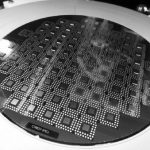
Our EDA industry loves three letter acronyms so credit the same industry for creating a five letter acronym CoWoS. Two weeks ago TSMC announced tape-out of their first CoWoS test chip integrating with JEDEC Wide I/O mobile DRAM interface, making me interested enough to read more about it. At the recent TSMC Open Innovation Platform there was a presentation from John Park, Methodology Architect at Mentor Graphics called –A Platform for the CoWoS Reference Flow. Continue reading “Chip On Wafer On Substrate (CoWoS)”
SpyGlass IP Kit 2.0

On Halloween, Atrenta and TSMC announced the availability of SpyGlass IP Kit 2.0. IP Kit is a fundamental element of TSMC’s soft IP9000 Quality Assessment program that assesses the robustness and completeness of soft (synthesizable) IP.
IP Kit 2.0 will be fully supported on TSMC-Online and available to all TSMC’s soft IP alliance partners on Nov. 20, 2012, just in time to make sure your turkey is SpyGlass Clean.
TSMC’s soft IP quality assessment program is a joint effort between TSMC and Atrenta to deploy a series of SpyGlass checks that create detailed reports of the completeness and robustness of soft IP. Currently, over 15 soft IP suppliers have been qualified through the program. IP Kit 2.0 represents an enhanced set of checks that adds physical implementation data (e.g., area, timing and congestion) and advanced formal lint checks (e.g., X-assignment, dead code detection). IP Kit 2.0 also allows easier integration into the end user’s design flow and enhanced IP packaging options.
On the same subject, IPExtreme had an all day meeting at the computer history museum about, duh, IP. One of the companies presenting was Atrenta and here is a video of Michael Johnson’s presentation on IP Kit.
And, completely off topic, at the end of the IPExreme event they served wine and beer and had a short presentation on each beforehand. Jessamine McLellan, then the sommelier at Chez TJ in Mountain View (now the bar manager at the not-yet-open Hakkasan in San Francisco) gave a presentation on pairing wine with food. That last name sounds a little familiar…
TSMC OIP Forum 2012 Trip Report!

The second annual TSMC Open Integration Platform Ecosystem Forum was last week and let me tell you it was excellent. Great update on the TSMC process technology road maps, great for networking within the fabless semiconductor ecosystem, great for seeing what’s new in EDA and IP, and great for SemiWiki. It was time well spent for sure. You can see my TSMC OIP 2011 trip report HERE for reference.
The opening video was excellent this year! It was all about collaboration of course and an orchestra is a perfect example. My wife played first chair violin so this theme really clicked with me. Last year’s theme was a rowing team which did not click with me. You can see the symphony videoHERE.
First up was Rick Cassidy. Rick is President of TSMC North America. Prior to joining TSMC in 1997 Rick was Vice President and General Manager of National Semiconductor’s Military and Aerospace Division. He joined National in 1979. Before that, Rick was an officer in the U.S. Army. He earned his Bachelor of Science degree from the United States Military Academy at West Point.
According to Rick attendance was up from last year which I certainly agree with. I counted 1008 seats in the main auditorium and estimate that 95% of them were taken. This does not include the partners manning the booths in the exhibition room next door.
Rick presented the TSMC vision and mentioned some interesting numbers:
*TSMC has more than 5,000 silicon validated IP available today, WOW! I have been through the TSMC silicon validation process many times and let me tell you it is rigorous to say the least.
*TSMC has invested $1.5B in design enablement thus far in 2012!
*TSMC in 1987 had one fab, a $20M CAPEX, 30 products and shipped 3,600 wafers
*TSMC in 2012 has 11 fabs, 5,498 different technologies, 12,569 products, $50B CAPEX, 615 customers, and a 15.3M wafer capacity!
Rick mentioned that his decision to join the semiconductor industry was based on the opportunity to change the world. I wish I could say the same. 30 years ago I was a starving college student and my decision was financial. I knew there was big money to be made in Silicon Valley and I wanted some. Looking back however we did change the world and there is still plenty of money to be made in doing so.
Next up was Dr. Mark Liu. Mark is TSMC’s Executive Vice President and Co-Chief Operating Officer. He joined TSMC in 1993 as an Engineering Manager. Prior to that Mark served in a number of technical capacities first with AT&T Bell Laboratories as a principal investigator in High Speed Electronics Research and later at Intel Corporation where he developed process technologies for Intel’s 32-bit microprocessors and flash memory products. Mark is a member of the Board of Directors of Silicon System Manufacturing Company in Singapore. He received Ph.D. degrees in electrical engineering and computer science from the University of California, Berkeley.
I met Mark when I toured Fab 12 in 2010, I blogged about it HERE. A memorable experience for sure. Mark ramped up TSMC’s first 200mm fab in 1993 and has been building fabs for TSMC ever since. Mark talked about “The Internet of Things” and what 2030 will look like. Mark also stated that:
*The TSMC 20nm design ecosystem (EDA and IP) are available today
*20nm is close to complete and will be in production next year
*TSMC will have three fabs for 20nm.
Next up was Dr. Cliff Hou, Cliff is vice president of R&D. Cliff’s door and mind is always open for new technology discussions and debates on the future of the semiconductor ecosystem. Cliff joined TSMC in 1997 and was appointed TSMC’s Vice President of Research and Development (R&D) in 2011. He was previously Senior Director of Design and Technology Platform where he established the company’s technology design kit and reference flow development organizations. He also led TSMC’s in-house IP development teams from 2008 to 2010. Cliff holds 20 U.S. patents and serves as a board member of Global Unichip Corp. He received his Ph.D. in electrical and computer engineering from Syracuse University.
Cliff added that:
*20nm engagements with partners and customers started much earlier
*TSMC overcame 20nm challenges through collaboration
*16nm FinFET will require even deeper collaboration
Cliff also mentioned that at 40nm partners and customers started design work when the PDK was release 0.5, at 28nm design work started at PDK 0.1, at 20nm design work started at PDK .05, and 16nm will start at PDK .01. The 20nm PDK 1.0 and 20nm foundation IP is silicon validated and available today with customer tape-outs expected in Q1 2013. 16nm PDK .1 will be available in Q1 2013 with the production version PDK 1.0 scheduled in Q4 2013.
The most interesting thing for me was the FinFET discussions and there were plenty of them which I will blog about separately. For those of you who don’t know about FinFETS start here with the FinFET Wiki. 2013 will be the year of the FinFET, absolutely!
TSMC dilemma: Cadence, Mentor or Synopsys?
Looking at the Press Release (PR) flow, it was interesting to see how TSMC has solved a communication dilemma. At first, let’s precise that #1 Silicon foundry has to work with each of the big three EDA companies. As a foundry, you don’t want to lose any customer, and then you support every major design flow. Choosing another strategy would be stupid.
The first PR came on October 12, about Chip on Wafer on Substrate tape out, here is an extract: “TSMC today announced that it has taped out the foundry segment’s first CoWoS™ (Chip on Wafer on Substrate) test vehicle using JEDEC Solid State Technology Association’s Wide I/O mobile DRAM interface… A key to this success is TSMC’s close relationship with its ecosystem partners to provide the right features and speed time-to-market. Partners include: Wide I/O DRAM from SK Hynix; Wide I/O mobile DRAM IP from Cadence Design Systems; and EDA tools from Cadence and Mentor Graphics.”
As you can see, both design tools from Cadence and Mentor are mentioned, and Cadence can be honored: the test vehicle is based on Wide I/O mobile DRAM IP from the company. We will have a look at Wide I/O more in depth soon in this blog.
Cadence and Mentor? Look like one is missing!
Then, today, the industry was awarded that Synopsys has “received TSMC’s 2012 Interface IP Partner of the Year Award for the third consecutive year. Synopsys was selected based on customer feedback, TSMC-9000 compliance, technical support excellence and number of customer tape-outs. Synopsys’ DesignWare Interface IP portfolio includes widely used protocols such as USB, PCI Express, DDR, MIPI, HDMI and SATA that are offered in a broad range of processes from 180 nanometer (nm) to 28nm.”
If you want to know more about the Interface IP market, weighting over $300 million in 2011, you should take a look at this post
The PR about the Chip on Wafer on Substrate (CoWoS) from TSMC shows that Cadence invests to develop the memory controller technology of the near future, to be used for 3D-IC on mobile applications. I suggest you to read this excellent article from Paul McLelan, so you will understand how work CoWoS from a Silicon technology standpoint.
I will rather focus on the Wide I/O Memory Controller. Here is the description of the key features, as described by Cadence:
Key Features
- Supports Wide I/O DRAM memories compliant with JESD229
- Supports typical 512-bit data interface from SoC to DRAM (4 x 128 bit channels) over TSV at 200MHz offering more than 100Gbit/sec of peak DRAM bandwidth
- Independent controllers for each channel allow optimization of traffic and power on a per-channel basis
- Supports 3D-IC chip stacking using direct chip-to-chip contact
- Supports 2.5D chip stacking using silicon interposer to connect SoC to DRAM
- Priority and quality-of-service (QoS) features
- Flexible paging policy including autoprecharge-per-command
- Two-stage reordering queue to optimize bandwidth and latency
- Coherent bufferable write completion
- Power-down and self-refresh
- Advanced low-power module can reduce standby power by 10x
- Supports single- and multi-port host busses (up to 32 busses with a mix of bus types)
- Priority-per-command (AXI4 QoS)
- BIST algorithm in hardware enables high-speed memory testing and has specific tests for Wide I/O devices
It’s amazing! During the last ten years, we have seen a massive move from parallel to serial interface, think about PCI moving to PCI Express, PATA being completely replaced by SATA in storage application in less than 5 years, and the list is long. With the Wide I/O concept, we can see that a massively (512-bit) parallel interface, running at 200 MHz (to be compared with LPDDR3 at 800 MHz DDR), can offer both a better bandwidth up to 17 GB/s, and a better power per transfer performance than LPDDRn solution.
Anything magic here? The higher performance in term of bandwidth can be easily explained: adding enough 64-bit wide busses will allow passing LPDDR3 performance. But the reason why the power per transfer is better is more subtle: because it’s a 3D technology, the connection between the SoC and the DRAM will be made in the 3[SUP]rd[/SUP] (vertical) dimension, as shown in the picture from Qualcomm : thus, the connection length will be shorter than any connection made on a board. Moreover, the capacitance (due to the bumping or bonding material and to the track on the PCB) will be minimized with 3D connection. Then the power per bit transferred at a certain frequency. I did not checked how this was computed, but I am not shocked by this result…
So, Wide I/O memory controller looks like a superb new technology developed by Cadence, the mobile market is healthy enough (an understatement!) to decide to introduce the technology, but, as mentioned by Qualcomm on the above picture “Qualcomm want this but also competitive pricing”…
Eric Esteve from IPNEST
Soft IP Quality Standards

As SoC design has transformed from being about writing RTL and more towards IP assembly, the issue of IP quality has become increasingly important. In 2011 TSMC and Atrenta launched the soft IP qualification program. Since then, 13 partners have joined the program.
IP quality is multi-faceted but at the most basic level, an IP block needs to do two things: it needs to meet its specification (for example, adhering to the protocol standard for a network interface) and it needs to be easy to implement into the design. Ideally, the IP itself does not need to be changed at all, this would be an indication of lack of IP quality and immediately increases the verification cost.
October 16th is the TSMC Open Innovation Platform Ecosystem Forum at the San Jose convention center. Anuj Kumar of Atrenta will discuss the TSMC IP Kit, which is a joint development between TSMC and Atrenta using the SpyGlass platform for IP handoff analysis and validation. The presentation will be at 11am. In particular he will discuss the new version of the IP Kit, TSMC IP Kit 2.0, currently under joint development between Atrenta and TSMC. This version of the kit adds physical analysis of the IP (such as routing congestion) as well as advanced formal metrics the explore the ease of verification of the IP.
Anuj will review the tests that are part of the Kit, show example quality metrics and DataSheet reports, and discuss the kind of design issues that have been uncovered and fixed as a result of the program. He will present the timeline for implementation of IP Kit 2.0 and the results of the testing of IP Kit V2.0 with IP partners.
Information about the TSMC OIP Ecosystem Forum is here. Information about IP Kit is here. As well as Anuj presenting, Atrenta will also be exhibiting at booth #405.
TSMC OIP Ecosystem Forum 2012

The TSMC Open Innovation Platform® (OIP) Ecosystem Forum brings TSMC’s design ecosystem member companies together to share with our customers real-case solutions for customers’ design challenges and success stories of best practice in TSMC’s design ecosystem.
More than 90% of the attendees last year said “this forum helped them better understand the components of TSMC’s Open Innovation Platform” and “they found it effective to hear directly from TSMC OIP member companies.”
Please introduce yourself if you see me. It would be a pleasure to meet you!
REGISTRATION
This year, the forum will feature a day-long conference starting with executive keynotes from TSMC and ARMin the morning plenary session to outline future design challenges and roadmaps, as well as discuss a recent collaboration announcement, 30 selected technical papersfrom TSMC’s EDA, IP, Design Center Alliance and Value Chain Aggregator member companies, and an Ecosystem Pavilion featuring up to 80 member companies showcasing their products and services.
Agenda
San Jose Convention Center,
Tuesday , October 16th, 2012
[TABLE] cellpadding=”4″ style=”width: 97%”
|-
| colspan=”4″ align=”center” | Plenary Session
|-
| style=”width: 15%” | 08:00
| colspan=”3″ | Registration Opens
|-
| 09:00 – 09:10
| colspan=”2″ | Welcome Remarks
| style=”width: 29%” | TSMC NA Executive
|-
| 09:10 – 09:40
| colspan=”2″ | An Ecosystem for Innovation
| TSMC Executive
|-
| 09:40 – 10:10
| colspan=”2″ | TSMC Design Technology Update
| TSMC Executive
|-
| 10:10 – 10:40
| colspan=”2″ | ARM Feature Talk
| Inviting Executive Level Speaker
|-
| 10:40 – 11:00
| colspan=”3″ align=”center” | Coffee Break
|-
[TABLE] cellpadding=”4″ style=”width: 97%”
|-
| align=”center” style=”width: 15%” | [TABLE] cellpadding=”10″ style=”width: 100%”
|-
| align=”center” |
|-
| align=”center” width=”27%” | EDA Track
| align=”center” width=”29%” | IP Track
| align=”center” width=”29%” | EDA/IP/Services Track
|-
| 11:00 – 11:30
| align=”center” valign=”top” | [TABLE] cellspacing=”3″ style=”width: 100%”
|-
| align=”center” valign=”top” | A Platform for the CoWoS Reference Flow
|-
| align=”center” valign=”top” | Mentor Graphics
|-
| align=”center” valign=”top” | [TABLE] cellspacing=”3″ style=”width: 100%”
|-
| align=”center” valign=”top” | TSMC IP Kit V2.0 – Enhancing Soft IP Quality Standards
|-
| align=”center” valign=”top” | Atrenta
|-
| align=”center” valign=”top” | [TABLE] cellspacing=”3″ style=”width: 100%”
|-
| align=”center” valign=”top” | SiP, 3D-IC & IPD Complement Flexible ASICs
|-
| align=”center” valign=”top” | GUC
|-
|-
| 11:30 – 12:00
| align=”center” valign=”top” | [TABLE] cellspacing=”3″ style=”width: 100%”
|-
| align=”center” valign=”top” | How to Manage Variability and Double
Patterning at 20nm
|-
| align=”center” valign=”top” | Cadence
|-
| align=”center” valign=”top” | [TABLE] cellspacing=”3″ style=”width: 100%”
|-
| align=”center” valign=”top” | 1T-OTP – Non-Volatile Memory for
Mobile and Other Low-Power Applications
|-
| align=”center” valign=”top” | Sidense
|-
| align=”center” valign=”top” | [TABLE] cellspacing=”3″ style=”width: 100%”
|-
| align=”center” valign=”top” | Timing Sign-off and Technology Migration Using Functionalized Timing Reports
|-
| align=”center” valign=”top” | IMEC
|-
|-
| 12:00 – 12:30
| align=”center” valign=”top” | [TABLE] cellspacing=”3″ style=”width: 100%”
|-
| align=”center” valign=”top” | Finding and Fixing Double Patterning Errors in 20nm Design
|-
| align=”center” valign=”top” | Mentor Graphics &
TSMC
|-
| align=”center” valign=”top” | [TABLE] cellspacing=”3″ style=”width: 100%”
|-
| align=”center” valign=”top” | Implementing and Optimising Graphics IP in SoCs
|-
| align=”center” valign=”top” | Imagination Technologies
|-
| align=”center” valign=”top” | [TABLE] cellspacing=”3″ style=”width: 100%”
|-
| align=”center” valign=”top” | Truly Differentiated Memory Subsystems on TSMC’s Advanced Technology Nodes
|-
| align=”center” valign=”top” | eSilicon
|-
|-
| 12:30 – 13:30
| colspan=”3″ align=”center” valign=”top” | Lunch
|-
| 13:30 – 14:00
| align=”center” valign=”top” | [TABLE] cellspacing=”3″ style=”width: 100%”
|-
| align=”center” valign=”top” | Enabling 20nm Custom Design in Laker
|-
| align=”center” valign=”top” | Springsoft
|-
| align=”center” valign=”top” | [TABLE] cellspacing=”3″ style=”width: 100%”
|-
| align=”center” valign=”top” | Advanced Silicon Design Methodology For Achieving 20nm Ready, Physical IP
|-
| align=”center” valign=”top” | Synopsys
|-
| align=”center” valign=”top” | [TABLE] cellspacing=”3″ style=”width: 100%”
|-
| align=”center” valign=”top” | Publishing Innovation through IP Targeting TSMC Technology
|-
| align=”center” valign=”top” | Design & Reuse
|-
|-
| 14:00 – 14:30
| align=”center” valign=”top” | [TABLE] cellspacing=”3″ style=”width: 100%”
|-
| align=”center” valign=”top” | 3D-IC Silicon Interposer IC Design Flow Using Cadence Encounter Digital Implementation (EDI) System
|-
| align=”center” valign=”top” | Cadence
|-
| align=”center” valign=”top” | [TABLE] cellspacing=”3″ style=”width: 100%”
|-
| align=”center” valign=”top” | Comprehensive Embedded NVM Solution in Trusted Technology and Capacity Platform
|-
| align=”center” valign=”top” | eMemory
|-
| align=”center” valign=”top” | [TABLE] cellspacing=”3″ style=”width: 100%”
|-
| align=”center” valign=”top” | TMI: A Unified Compact Model Development Platform for 28nm & Beyond
|-
| align=”center” valign=”top” | Synopsys &
TSMC
|-
|-
| 14:30 – 15:00
| align=”center” valign=”top” | [TABLE] cellspacing=”3″ style=”width: 100%”
|-
| align=”center” valign=”top” | Verification of Power, Signal, and Reliability Integrity for 3D-IC/Silicon Interposer Designs
|-
| align=”center” valign=”top” | ANSYS / Apache
|-
| align=”center” valign=”top” | [TABLE] cellspacing=”3″ style=”width: 100%”
|-
| align=”center” valign=”top” | Novel Low-Power Audio CODEC from 180nm to 28nm with Moore and More!
|-
| align=”center” valign=”top” | Dolphin Integration
|-
| align=”center” valign=”top” | [TABLE] cellspacing=”3″ style=”width: 100%”
|-
| align=”center” valign=”top” | Design Methodology for Silicon-Accurate Jitter Analysis for 28nm Interface IP for 100GB Applications
|-
| align=”center” valign=”top” | Berkeley Design Automation &
Analog Bits
|-
|-
| 15:00 – 15:30
| colspan=”3″ align=”center” | Coffee Break
|-
| 15:30 – 16:00
| align=”center” valign=”top” | [TABLE] cellspacing=”3″ style=”width: 100%”
|-
| align=”center” valign=”top” | TSMC Certification for Cadence 20nm RTL-to-GDSII Flow
|-
| align=”center” valign=”top” | Cadence
|-
| align=”center” valign=”top” | [TABLE] cellspacing=”3″ style=”width: 100%”
|-
| align=”center” valign=”top” | Solving ESD, EOS and Latch-Up Requirements
– For Analog Interfaces in Advanced CMOS
– For Automotive Applications in TSMC’s BCD Platforms
|-
| align=”center” valign=”top” | SOFICS
|-
| align=”center” valign=”top” | [TABLE] cellspacing=”3″ style=”width: 100%”
|-
| align=”center” valign=”top” | Comprehensive Simulation and Modeling Solutions for TSMC’s RF Platforms
|-
| align=”center” valign=”top” | Agilent / EEsof
|-
|-
| 16:00 – 16:30
| align=”center” valign=”top” | [TABLE] cellspacing=”3″ style=”width: 100%”
|-
| align=”center” valign=”top” | Double-Patterning Technology and Impact on 20nm Designs
|-
| align=”center” valign=”top” | Synopsys
|-
| align=”center” valign=”top” | [TABLE] cellspacing=”3″ style=”width: 100%”
|-
| align=”center” valign=”top” | Enabling Design with Advanced Node Design IP for TSMC
|-
| align=”center” valign=”top” | Cadence
|-
| align=”center” valign=”top” | [TABLE] cellspacing=”3″ style=”width: 100%”
|-
| align=”center” valign=”top” | Silicon-Accurate Mixed-Signal Fractional-N PLL IP Design
|-
| align=”center” valign=”top” | Berkeley Design Automation &
Silicon Creations
|-
|-
| 16:30 – 17:00
| align=”center” valign=”top” | [TABLE] cellspacing=”3″ style=”width: 100%”
|-
| align=”center” valign=”top” | Improved Design for Reliability Using Calibre PERC
|-
| align=”center” valign=”top” | Mentor Graphics
|-
| align=”center” valign=”top” | [TABLE] cellspacing=”3″ style=”width: 100%”
|-
| align=”center” valign=”top” | Kilopass Roadmap for Advanced TSMC Processes
|-
| align=”center” valign=”top” | Kilopass
|-
| align=”center” valign=”top” | [TABLE] cellspacing=”3″ style=”width: 100%”
|-
| align=”center” valign=”top” | Chip-Partitioning Trends in Systems Using Ultra Deep-Submicron SoCs
|-
| align=”center” valign=”top” | Cosmic Circuits
|-
|-
| 17:00 – 17:30
| align=”center” valign=”top” | [TABLE] cellspacing=”3″ style=”width: 100%”
|-
| align=”center” valign=”top” | Automated Approach for Waiving Physical Verification Errors at IP
|-
| align=”center” valign=”top” | Mentor Graphics &
LSI
|-
| align=”center” valign=”top” | [TABLE] cellspacing=”3″ style=”width: 100%”
|-
| align=”center” valign=”top” | Using Latest-Generation DDR4, LPDDR3 and
Wide-IO DRAM Devices with Chips in TSMC’s
Advanced 28nm and 20nm Processes
|-
| align=”center” valign=”top” | Cadence
|-
| align=”center” valign=”top” | [TABLE] cellspacing=”3″ style=”width: 100%”
|-
| align=”center” valign=”top” | CMOS Silicon Millimeterwave Design Closure on
Integrated Fullwave Electromagtic Simulation and
Extraction Platform with a Real Silicon Design Case
|-
| align=”center” valign=”top” | Lorentz &
Stanford University
|-
|-
| 17:30 – 18:00
| colspan=”3″ align=”center” | Networking and Reception
|-
Legal Notice:TSMC is not responsible for the content, accuracy, or reliability of any of the presentations at the TSMC Open Innovation Platform Ecosystem Forum. Furthermore, posting the presentation abstracts on TSMC’s corporate website does not constitute an endorsement of the content of those presentations by TSMC. Any liability arising from the contents of any of the presentations is the responsibility of the presenter itself, and not TSMC.
Exclusive Sneak Peek: Cadence at TSMC OIP Ecosystem Forum 2012

The TSMC Open Innovation Platform® (OIP) Ecosystem Forum brings TSMC’s design ecosystem member companies together to share with our customers real-case solutions for customers’ design challenges and success stories of best practice in TSMC’s design ecosystem. More than 90% of the attendees last year said “this forum helped them better understand the components of TSMC’s Open Innovation Platform” and “they found it effective to hear directly from TSMC OIP member companies.”
Cadence and TSMC have a long history of collaborating to deliver solutions that ensure our joint customers’ success. Along with design ecosystem partners such as ARM, Cadence and TSMC team up on TSMC’s Open Innovation Platform to optimize design and manufacturing efficiencies to ensure your design’s success.
While at TSMC OIP 2012, be sure to schedule your time to catch all the activities and sessions that Cadence is hosting. Here is your schedule for all things Cadence at OIP.
At 12:30, enjoy lunch courtesy of Cadence, your official lunch sponsor for TSMC OIP 2012.
After the morning keynotes, Cadence will deliver detailed technical sessions in both the IP and EDA tracks.
- 11:30 AM: How to Manage Variability and Double Patterning at 20nm (EDA track)
- 2:00 PM: 3D-IC Silicon Interposer IC Design Flow Using Cadence Encounter Digital Implementation (EDI) System (EDA track)
- 3:30 PM: TSMC Certification for Cadence 20nm RTL-to-GDSII Flow (EDA track)
- 4:00 PM: Enabling Design with Advanced Node Design IP for TSMC (IP track)
- 5:00 PM: Using Latest-Generation DDR4, LPDDR3 and Wide-IO DRAM Devices with Chips in TSMC’s Advanced 28nm and 20nm (IP track)
Cadence demonstrations will be available throughout the day. Visit Cadence in Booth 414 to see demonstrations of how Cadence and TSMC collaborate to help you optimize PPA. Demonstrations include:
- 3D-IC Design Infrastructure Enablement Supporting CoWoS
- Virtuoso 20nm Certified Technologies
- 20nm Certified High Performance Technologies
- Custom Design Qualified Reference Flow
- Certified Signoff Technologies for Advanced Nodes
- Design IP for DDR4 and 28nm
Win a Kindle Fire Visit two demo stations in Cadence booth 414 and have your entry form from your registration bag stamped at each demo station. Drop off your completed entry form at Cadence booth 414 before 6:00PM. The winner will be drawn before the end of the networking reception.
Will Paul Otellini Convince Tim Cook to Fill Intel’s Fabs?
An empty Fab is a terrible thing to waste, especially when it is leading edge. By the end of the year Intel will, by my back of the envelope calculation, be sitting with the equivalent of one idle 22nm Fab (cost $5B). What would you do if you were Paul Otellini?
Across the valley, in Cupertino, you have Tim Cook, whose modus operandi is to scour the world for underutilized resources and plug them into the ever-growing Apple Keiretsu at below market prices. It’s always time to go more vertical.
With the launch of the iphone 5 behind him and the supply chain ramped to deliver 50MU of iPhone 5 in Q4, there seems to be a silly game in the press of how to raise Tim’s dander on all that is wrong in the Apple ecosphere. The component shortages that exist today are in reality the flip side of the coin known as unlimited demand at Day 1 of the new product launch. However, with Samsung ever on Apple’s heals, the game doesn’t stop and Apple must continue to innovate as well as wring out supply chain inefficiencies. The one that, no doubt, is staring Cook in the eye for 2013 is the A6 processor currently in production in Samsung’s Austin Fab. It is the last major component being produced by Samsung and it needs to move to a friendlier foundry.
For months the rumor mills have been rattling with stories of a TSMC – Apple partnership at 20nm targeting first production the end of 2013. This seems logical, given that Apple is moving to a two-supplier model across most of its major components. If they were to continue with this strategy, then it would mean they have to pick up another foundry (i.e. Global Foundries or Intel) to go hand in hand with TSMC and avoid any single point of failure due to “Acts of God” or unforeseen upside, both of which we have seen the past 24 months.
Intel’s announcement a couple weeks ago on a PC slowdown in Q3 came with a hint that 22nm is yielding well. If, however Intel’s revenues going forward are flat or even slightly rising as opposed to the 24% growth they experienced in both 2010 and 2011 then the Fab expansion plans they outlined last year regarding 22nm and 14nm would raise the question – for what reason? Perhaps it was the only strategy that Otellini could logically employ as Intel tries to outrun TSMC and Samsung.
A year ago, there were doubts as to whether Intel’s new 22nm Finfet process would yield as well as previous process technologies. If the PC market and the DataCenter continued to grow as in past years and if Ivy Bridge were to cannibalize the graphics cores of AMD and nVidia, then the argument could be made to expand Intel’s 22nm Fab footprint from 3 to 4. And so it is expected at year-end the 4[SUP]th[/SUP] Fab will come on line while Intel is swimming in well yielding Ivy Bridges. Look out below AMD and nVidia, your days may be numbered in a soft PC market.
The addition of two mammoth 14nm Fabs that can be upgraded to 450mm to Intel’s capex budgets seems to speak of insanity, unless they expect them to come on line much sooner and that it truly does represent a 4 year lead over competitors. Mark Bohr at IDF mentioned that 14nm will be ready for production the end of 2013 and word is that the 14nm successor to Haswell, called Broadwell, is already up and running Windows. This begs the question, is Broadwell really two years away from production or will Intel launch it early, thus setting up a 22nm to 14nm Fab transition 2H 2013? Otellini would seem to be in a position to deploy his large, highly efficient 22nm Aircraft Carriers in any number of Foreign Oceans wreaking havoc. Or perhaps, aggressively leverage them for a long-term fab deal with Apple.
If Otellini were to offer Apple free wafers, would Tim Cook disregard it? Preposterous you say. OK, but this is what game theory is all about. You have to test the limits and I believe until the summer slowdown, Otellini’s bid to Apple was to sell wafers with a 60% margin markup.
In this new environment, Otellini will be more likely to offer a price that is closer to cost plus a small adder for anytime starting first half 2013 and extending thru 2015. What are the ramifications for Apple? The new A6 processor is a 95mm die in Samsung’s 32nm process and costs somewhere around $25 (I have seen estimates from $18 to $28). In round numbers the A6 in Intel’s 22nm process is 50mm in size. If Intel saves Apple $10 a chip, then it is equivalent to $3B a year (300MU) that drops to its Operating line and would add nearly $50 to Apple’s stock price (based on 15.5 P/E).
The overriding issue for Intel and Paul Otellini is, as I mentioned before, that they need to move to 14nm as quickly as possible and take as much of the market with them (both x86 and Apple) and thereby eliminate the threat posed by TSMC and Samsung as Foundries looking to supply a greater percentage of the total semiconductor market that is built in leading edge processes. Until the last couple years, Intel consistently had over 90% of the leading edge compute semiconductor content delivered with their x86 processors, a legacy that goes back to the transition of IBM mainframes to the Desktop PC.
The End Game continues to get more interesting as we get closer to “All In with Leading Edge.”
Full Disclosure: I am Long AAPL, INTC, QCOM and ALTR
Mentor Graphics Update at TSMC 2012 OIP

What
In just 20 days you can get an update on four Mentor Graphics tools as used in the TSMC Open Innovation Platform (OIP). Many EDA and IP companies will be presenting along with Mentor, so it should be informative for fabless design companies in Silicon Valley doing business with TSMC.
Continue reading “Mentor Graphics Update at TSMC 2012 OIP”
Taiwan Travel Explained!
Whenever people hear that I travel internationally one week a month they cringe at the thought of crowded airports, 12 hour flights, jet lag, and days packed with meetings. I generally shrug, accept the label of travel warrior, and say it is all part of doing business in the semiconductor ecosystem. But in reality, it is not as bad as it sounds, especially if you include the knowledge gained as part of the ROI calculation.
First and foremost, I rarely travel alone. As a business consultant I work for the CEOs of emerging technology companies advising them on a variety of topics. I wish I could say they learn more from me than I do from them but that is rarely the case. Successful emerging technology CEOs are a unique breed and are almost always a pleasure to work with. These CEOs wear so many hats and work so many hours that I get a headache just thinking about it. Every trip brings new problems and new ways to solve them which is an excellent learning experience on many different levels.
As a frequent traveler, I get perks from airlines and hotels fit more for a king than a regular working person. Executive lounges at airports are a good example. Right now I’m in the EVA airlines Evergreen Lounge sipping champagne and eating rice crispy treats (I don’t like caviar). Seat upgrades, personalized in-flight service, priority baggage handling etc…, it really does take the sting out of air travel. Even the airport garage I park my car in has frequent parking perks: Car washes, oil changes, priority shuttle services etc…
The hotels are the most generous. I get corporate rates for the cheapest rooms and the upgrades just keep coming. The rooms I usually get are huge with every modern convenience you can imagine. Sometimes the bathrooms are absolutely amazing. As you approach the toilet the seat raises, auto flushes, washes and dries, and closes as you walk away, semiconductor technology at its finest! The hotel welcome baskets are quite tasty and quite fattening, so I always bring my gym clothes to burn the extra calories that come with travel. Exercise also helps with jet lag. Another way I avoid jet lag is to NOT eat airline food and drink lots of water, believe it.
The boxes in the picture are Taiwan tea which is an interesting story in itself. A fellow international traveler convinced me that green tea is the key to a long and fruitful life and I have been drinking it ever since. That was more than ten years ago and I still believe it. I started with Japanese green tea but now Taiwan tea is my favorite.
In the hills right above the TSMC fabs in Hsinchu Science Park is one of the more famous green tea farms which I visit quite frequently. As the Taiwanese tea legend goes:
A tea farmer’s crop was infested by little green-leaf worms. Trying to recover from this catastrophic loss, the tea farmer went into town to sell his low-grade tea anyway. As it turns out the tea had a unique flavor and gained huge popularity. This guy was a great salesman for sure! When the tea farmer returned to his village and told the story it was viewed as bragging so they called his tea “puffing tea”, puffing means bragging in Taiwanese. The legend also says that Puffing Tea was a favorite of Britain’s Queen Victoria (1800’s) and she gave it the name Oriental Beauty Tea. European aristocrats later named it Champion Oolong Tea.
The tea is harvested three times a year. In the spring it is green tea (the green box) which has a mild flavor. Next harvest is orange tea. Fall harvest is red tea with the strongest flavor. If you look on the top of the boxes there are pictures of green-leaf worms which determines the price. The more worms the higher the price. There is more on Taiwan Tea Farms HERE. Even though Starbucks has invaded every corner of Taiwan, tea is still a big part of modern life here.