Cliff Hou of TSMC gave the keynote today at SNUG on Collaborate to Innovate: a Foundry’s Perspective. Starting around 45nm the way that a foundry has to work with its ecosystem fundamentally changed. Up until then, each process generation was similar enough to the previous one, apart obviously from size, that it could be designed with the EDA tools already out there. Yes, new factors like signal integrity would grow in importance but this happened over several process generations and so was incremental. Basically, designers would wait for the first release of the Spice decks and the DRC rule decks and then get going.
This doesn’t work any more. Since then each process generation has a major discontinuity:
- 45nm: power must be addressed
- 28nm: high-K metal gate
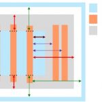
- 20nm: double patterning
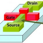
- 16nm: FinFET
- 10nm: multiple patterning and spacer
These discontinuities mean that foundries such as TSMC have to work closely with EDA suppliers such as Synopsys to ensure that the tools are ready when the process is ready. Otherwise they face the problem of building a $5B fab and not having any designs ready to run in it for a year. For example, without double patterning aware place & route, and layout editors, DRCs etc it is not possible to do a 20nm design.
This is happening in an environment where the number of tapeouts is not increasing, and is probably declining. But the number of wafers needed in production is increasing exponentially. This makes it critically important to hit the volume and yield-learning ramps for a new process. Wafers that are not manufactured don’t really come back, the end-user will have purchased another product. TSMC is increasing its capacity at a 31% CAGR. That’s a lot of wafer starts. Better make sure there are really wafers to start.
Another factor that has been growing in importance is the increasing use of IP in SoC designs. This means that not only do EDA tools need to be ready to go when the process is ready, but IP needs to be ready too. It is hard to do an SoC design without DDRx, PCIe, USB and so on.
So TSMC needs to have 3 parallel collaboration tracks:
- working with EDA suppliers to ensure that the gotcha new features such as double patterning or FinFETs in the new process have full support in the tools
- working with IP suppliers to ensure that IP is ready in a timely manner. It may not be possible to have all IP available when the process is ready, for both technical (IP suppliers need the tools and the process to be reasonably stable to get work done) and economic (there is a lot of IP and it can’t all be created in parallel
- working with lead design groups to ensure that the process matches their needs, that they have the PDKs and design kits they require and so on
The goal is to have everything come together so that when the process is ready and the fab is ready to ramp to volume, that the designs are there. In turn that requires IP and tools to be there to get the designs done.
The next process, 16nm, is a FinFET process so the new challenges largely are around the transistors (the metal fabric is basically unchanged from 20nm). Although FinFETs are wonderful from some points of view (low leakage, high current, lower voltage) they have some disadvantages too (higher parasitic capacitance, higher parasitic resistance due to the MEOL local interconnect, quantized device widths). The biggest challenge has probably been RC extraction accuracy, although that seems to be as good with FinFET as at 28nm now.
The goal for future processes is:
- around 2X increase in gate-density per node. With no EUV at 10nm this will get challenging
- 15% speedup with 25% power reduction per node. This should be easier than the area reduction
- And although Cliff didn’t mention it, another major challenge is to keep the cost per wafer in line so that the 2X increase in gate-density also shows up as a cost reduction
So collaboration within the TSMC Open Innovation Platform (OIP) is the only way to address these types of challenge and get everyone to the finish line at the same time.
And with that, Cliff Hou went to get on a plane back to Taiwan having only flown in yesterday!