TSMC Technologies for Mobile and HPC

TSMC Technologies for Mobile and HPC
by Alex Tan on 05-10-2018 at 12:00 pm

During TSMC 2018 Technology Symposium, Dr. B.J. Woo, TSMC VP of Business Development presented market trends in the area of mobile applications and HPC computing as well as shared TSMC progress in making breakthrough efforts in the technology offerings to serve these two market segments.

Both 5G and AI are taking the center stage in shaping the high double-digit data growth demand. For mobile segment, the move from 4G LTE to 5G requires the use of higher modem speed (from 1Gbps to 10Gbps), 50% faster CPU, twice faster GPU, double transistor density, 3X performance increase of AI engines to 3 TOPS (Trillion Operations Per Seconds) target and without much power increase. In this market segment, TSMC is ushering the move from 28HPC+ towards 16FFC.

On the cloud side, data center switch demands double throughput, from 12.8Tbps to 25.6Tbps as the computing demand move towards the network edge. Similarly the drive towards double memory bandwidth, 3 to 4x increase in throughput of AI accelerators and up to 4x transistor density improvement are taking place.

N7 Technology Progress
Dr. Woo stated that delivering high density and power efficiency requirements to satisfy low latency of data intensive AI application is key to the success of TSMC N10 process. It has also enabled AI in the smartphones space. On the sideline, N7 node has been making good progress in providing excellent PPA values with >3x density improvement, >35% speed gain and >65% power reduction over its 16nm predecessor.

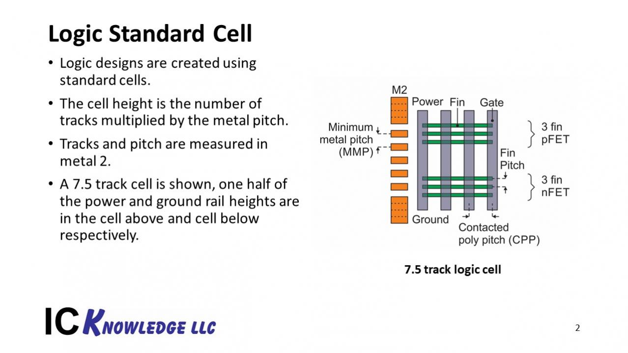
N7 HPC track provides 13% speed over N7 mobile (7.5T vs 6T), while it has passed the yield and qual tests (SRAM, FEOL, MEOL, BEOL) and MP-ready D0. Part of the contributing factor is TSMC successful leveraged learning from N10 D0 and it is targeted for Fab15.

The N7 IP ecosystem is also in ready state with over 50 tapeouts slated by end of 2018 for mobile, HPC, automotive and servers. The 7nm technology is anticipated to be having a long life similar to its predecessor 28nm/16nm nodes. The combination of mild pitch scaling from N10 to N7 plus the migration from immersion to EUV scaling and denser standard cell architecture make significant overall improvement.

EUV Adoption and N7+ Process Node
She shared some progress of the EUV application on N7+. Applicable on selected layers, EUV reduces the process complexity and enhances resulting pattern fidelity. It also enables future technology scaling while offering better performance, yield and shorter cycle time. Dr. Woo showed caption of via resistance having much tighter distribution in N7+ EUV versus N7+ immersion as it delivers better uniformity.

The N7+ value proposition includes delivering 20% more logic density over N7, 10% lower power at same speed, and additional performance improvements anticipated from the ongoing collaboration with customers.

N7+ will also have double digit good die increase over N7 node as it gains traction from capitalizing the use of the same equipment and tooling. She claimed that it has lower defect density than other foundries as well as comparable 256Mb SRAM yield and device performance vs N7 baseline. TSMC provides easy IP porting (layout and re-K) from N7 to N7+ for those design entities that do not need to be redesigned.

HPC and N7+ Process Node
For HPC platform solution, the move from N7 to N7+ involves the incorporation of EUV, denser standard cell architecture, ultra-low Vt transistors, high-performance cells, SHDMIM (Super High Density MIM) capacitance and larger CPP (Contacted Poly Pitch) and 1-fin cells.

N7+ offers better performance and power usage through the use of an innovative standard cell architecture. It allows higher fin density in the same footprint for 3% speedup. On the other hand, reducing power by applying single-fin in non-timing-critical area reduces about 20% capacitance and in-turns, the dynamic power number.

The adoption of new structures also enhances MIM capacitance and utilization rate for HPC 3% to 5% performance boost. N7+ design kit is ready for supporting the IP ecosystem.

N5 Value Proposition
It has new elVt (extreme low Vt) offering a 25% max speed-up versus N7, incorporating aggressive scaling and full-fledged EUV. N5 has made good progress with double digit yield on 256Mb SRAM. Risk production is slated to be 1H2019.

Dr. Woo also shared a few metrics compared with N7 process (test vehicles used ARM A72 CPU core + internal ring oscillator):
– 15% speed improvement (up to 25% max speed)
– 30% power reduction
– 1.8x increased logic density through innovative layout and routing
– 1.3x analog density improvement through poly pitch shrink and selective Lg and fin #, yielding a more structured layout (“brick-like” patterns)

16FFC/12FFC Technologies
Dr. Woo covered RF technologies and roadmap (more on this in subsequent blog on IoT and Automotive). She mentioned that N16 and N12 FinFet based platform technologies have broad coverage, addressing HPC, mobile, consumer and automotive. Both 16FFC and 12FFC have shown strong adoption data with over 220 tapeouts. 12FFC should deliver 10% speed gain, 20% power reduction and 20% increased logic density vs 16FFC through dual-pitch BEOL, device boost, 6-track stdcell library and 0.5v VCCmin.

To recap, AI and 5G are key drivers for both mobile and HPC product evolutions. Along this line, TSMC keeps pushing the PPA (Power, Performance and Area) envelopes for the mainstream products while delivering leading RF technologies to keep pace with technology accelerated designs in these segments.

Also read: Top 10 Highlights of the TSMC 2018 Technology Symposium


Top 10 Highlights of the TSMC 2018 Technology Symposium

Top 10 Highlights of the TSMC 2018 Technology Symposium
by Tom Dillinger on 05-04-2018 at 12:00 pm

Here are the Top 10 highlights from the recent TSMC 2018 Technology Symposium, held in Santa Clara CA. A couple of years ago, TSMC acknowledged the unique requirements of 4 different market segments, which has since guided their process development strategy — Mobile, High-Performance Computing (HPC), Automotive, and IoT. Many of the highlights described below are in the context of a specific platform.
Continue reading “Top 10 Highlights of the TSMC 2018 Technology Symposium”


Leading Edge Logic Landscape 2018

Leading Edge Logic Landscape 2018
by Scotten Jones on 03-16-2018 at 2:00 pm

The most viewed blogs I write for SemiWiki are consistently blogs comparing the four leading edge logic producers, GLOBALFOUNDRIES (GF), Intel, Samsung (SS) and TSMC. Since the last time I compared the leading edge new data has become available and several new processes have been introduced. In this blog I will update the current status.
Continue reading “Leading Edge Logic Landscape 2018”


Webinar: Multiphysics Reliability Signoff for Next-Generation Automotive Electronics Systems

Webinar: Multiphysics Reliability Signoff for Next-Generation Automotive Electronics Systems
by Bernard Murphy on 02-08-2018 at 7:00 am

In case you missed the TSMC event, ANSYS and TSMC are going to reprise a very important topic – signing-off reliability for ADAS and semi-autonomous /autonomous systems. This topic hasn’t had a lot of media attention amid the glamor and glitz of what might be possible in driverless cars. But it now seems like the cold light of real engineering needs are advancing over the hype, if this year’s CES is any indication (see my previous blog on CES). Part of that engineering reality is ensuring not only that we can build these clever systems but that they will also continue to work for a respectable amount of time; in other words that they will be reliable, a topic as relevant for today’s advanced automotive electronics as it is for the systems of tomorrow.

REGISTER HERE for this event on February 22nd at 8am Pacific Time

This topic is becoming a pressing concern, especially for FinFET-based designs. There are multiple issues impacting aging, stress and other factors. Just one root-cause should by now be well-known – the self-heating problem in FinFET devices. In planar devices, heat generated inside a transistor can escape largely through the substrate. But in a FinFET, dielectric is wrapped around the fin structure and, since dielectrics generally are poor thermal conductors, heat can’t as easily escape leading to a local temperature increase, and will ultimately escape significantly through local interconnect leading to additional heating in that interconnect. Add to that increased Joule heating thanks to higher drive and thinner interconnect and you can see why reliability becomes important.

ANSYS has developed an amazingly comprehensive range of solutions for design for reliability, spanning thermal, EM, ESD, EMC, stress and aging concerns. In building solutions like this, they work very closely with TSMC, so much so that they got three partner of the year awards at the most recent TSMC OIP conference!

Incidentally my CES-related blog is here: https://www.legacy.semiwiki.com/forum/content/7274-ces-exhibitor-s-takeaway.html

Summary
Design for reliability is a key consideration for the successful use of next-generation systems-on-chip (SoCs) in ADAS, infotainment and other critical automotive electronics systems. The SoCs manufactured with TSMC’s 16FFC process are advanced multicore designs with significantly higher levels of integration, functionality and operating speed. These SoCs must meet the rigorous requirements for automotive electronics functional safety and reliability.

Working together, ANSYS and TSMC have defined workflows that enable electromigration, thermal and ESD verification and signoff across the design chain (IP to SoC to package to system). Within the comprehensive workflows, multiphysics simulations capture the various failure mechanisms and provide signoff confidence not only to guarantee first-time product success, but also to ensure regulatory compliance.

Attend this ANSYS and TSMC webinar to learn about ANSYS’ chip-package-system reliability signoff solutions for creating robust and reliable electronics systems for next-generation automotive applications, and to explore case studies based on TSMC’s N16FFC technology.

Founded in 1970, ANSYS employs nearly 3,000 professionals, many of whom are expert M.S. and Ph.D.-level engineers in finite element analysis, computational fluid dynamics, electronics, semiconductors, embedded software and design optimization. Our exceptional staff is passionate about pushing the limits of world-class simulation technology so our customers can turn their design concepts into successful, innovative products faster and at lower cost. As a measure of our success in attaining these goals, ANSYS has been recognized as one of the world’s most innovative companies by prestigious publications such as Bloomberg Businessweek and FORTUNE magazines.

For more information, view the ANSYS corporate brochure.


Machine Learning And Design Into 2018 – A Quick Recap

Machine Learning And Design Into 2018 – A Quick Recap
by Alex Tan on 02-07-2018 at 3:00 pm

How could we differentiate between deep learning and machine learning as there are many ways of describing them? A simple definition of these software terms can be found here. Let’s look into Artificial Intelligence (AI), which was coined back in 1956. The term AI can be defined as human intelligence exhibited by machines. While machine learning is an approach to achieve AI and deep learning is a technique for implementing subset of machine learning.


During last year 30-Year Anniversary of TSMC Forum, nVidia CEO Jen-Hsen Huang mentioned two concurrent dynamics disrupting the computer industry today, i.e.,how software development is done by means of deep learning and how computing is done through the more adoption of GPU as replacement to single-threaded/multi-core CPU, which is no longer scale and satisfy the current increased computing needs. The following charts illustrate his message.


At this month Santa Clara DesignCon2018 there were multiple well-attended sessions (2 panels and 1workshop) addressing Machine Learning Advances in Electronic Design. Highlighted by panelists coming from 3 different areas (EDA, industry and academia) were some successful snapshots of ML application in optimizing design and its potential consequences as how we should handle the generated models and methodologies.

From the industry:
Chris Cheng, a Distinguished Engineer from HPE presented a more holistic view of ML potential use coupled with test instruments as substitute for a software model based channel analysis. He also projected ML use to perform more proactive failure prediction of signal buses or complicated hardware such as solid-state drives.


Ken Wu, Google Staff HW Engineer shared his works on applying ML in channel modeling. He proposed the use of ML to predict channel’s eye-diagram metrics for signal integrity analysis. The learned models can be used to circumvent the need of performing complex and expensive circuit simulations. He believes ML opens an array of opportunity for channel modeling such as extending it to analyze the four-level pulse amplitude modulation (PAM-4) signaling, and the use of Deep Neural Network for Design of Experiment (DOE).

Dale Becker, IBM Chief Engineer of Electronic Packaging Integration, alluded to the potential dilemma imposed by ML. Does it supersede today’s circuit/channel simulation techniques, or is it synergistic? With the current design methodologies still reflecting heavy human interventions (such as in channel diagnostics, evaluation, optimization, physical implementation), ML presents an opportunity for exploration. On the other side of the equation, we need to be ready to address standardization, information sharing and IP protection.

From the EDA world, both Synopsys and Cadence were represented:

Cadence team — David White (Sr. Group Director), Kumar Keshavan (Sr. Software Architect) and Ken Willis (Product Engineering Architect) highlighted Cadence contribution in advancing ML adoption. David shared what Cadence has achieved with ML over the years on Virtuoso product and raised the crucial challenge of productizing ML. For a more in-depth coverage for David’s similar presentation on ML, please refer to another Wiki article TSMC EDA 2.0 With Machine Learning – Are We There Yet ? Kumar delved into Artificial Neural Network (ANN) concept and suggested its application for DOE of LPDDR4 bus. Ken Willis was moderating the afternoon panel and highlighted the recently introduced IBIS ML versus AMI model as well as impact of ML on solution space analysis.


Sashi Obilisetty, Synopsys R&D Director pointed out that the EDA ecosystem comprising of academic research, technology availability and industry interest) is ready and engaged. What we need is a robust, scalable, hi-performance and near real time data platform for ML application.

Several academia also shared their research progress under the auspice of Center for Advanced Electronics Through Machine Learning (CAEML) since its formation in 2016:

Prof. PaulFranzon discussed how ML could shorten IC physical design step through the use of surrogate model. The concept is to train a fast global model to evaluate from multiple evaluations of a detailed model that is slow to evaluate. Given an SOC design requiring a 40 minute per route iteration, the team needs about 50 runs to complete the Kriging based model overnight. Using this model, an optimal design can be obtained in 4 iterations which otherwise requires 20 iterations. The design has 18K gates derived from Cortex-M0 with 10ns cycle time and 45nm generic process.

Prof. Madhavan Swaminathan presented another application of ML based solution using surrogate model on channel performance simulation.

His view: Engineer (thinker) + ML (enabler) + Computers (doers) = enhanced solution. Extending ML into design optimization through active learning may ensure convergence to global optima and minimizing required CPU time.

With the increased design activities and research efforts in ML/DL applications, we should anticipate more coverage of such implementation into 2018. The next question would be if it will create a synergy and enhance design efforts through retooling and methodology adjustments, or it will create disruption that may change the human designer roles at different junctures of design capture. We should see.


TSMC 5nm and EUV Update 2018

TSMC 5nm and EUV Update 2018
by Daniel Nenni on 01-23-2018 at 12:00 pm

The TSMC Q4 2017 earnings call transcript is up and I found it to be quite interesting for several reasons. First and foremost, this is the last call Chairman Dr. Morris Chang will participate in which signifies the end of a world changing era for me and the fabless semiconductor ecosystem, absolutely. TSMC announced his retirement with Mark Liu, who has been co-CEO along with C.C. Wei since 2013, replacing Morris as Chairman and C.C. Wei taking over the role of single CEO. Earnings calls were much more interesting when Morris Chang participated especially in the Q&A session when he questioned some of the questions. Here is his good-bye:

I really have spent many years with some of you, many years, more than 20 years. Although I think most of you probably haven’t attended this particular conference that long. But having here almost 30 years I think, yes. And I enjoyed it, and I think that we all — at least I hope that I had a good time. I hope that you had a good time, too. And I will miss you, and thank you very, very much. Thank you. Thank you. Thank you.

The call started out with Laura Ho and financial recaps but also revenue by technology:

10-nanometer process technology continues to ramp strongly, accounted for 25% of total wafer revenue in the fourth quarter. The combined 16/20 contribution was 20% of total wafer revenue. Advanced technologies, meaning 28-nanometer and below, accounted for 63% of total wafer revenue, up from 57% in the third quarter. On a full year basis, 10-nanometer contribution reached 10% of total wafer revenue in 2017. The combined 16 and 20 contribution was 25% of total wafer revenue. Advanced technology, 28-nanometer and below, accounted for 58% of total wafer revenue, up from 54% in 2016.

This really is good news for TSMC since the more mature nodes (40nm and above) are more competitive thus lower margined. It will be interesting to see when TSMC lowers that advanced node bar below 28/22nm, probably in two years when 7nm hits HVM and 5nm is ramping.

Laura ended her remarks with a solid Q1 guidance:

Based on the current business outlook, we expect first quarter revenue to be between USD 8.4 billion and USD 8.5 billion, which is an 8.3% sequential decline but a 12.6% year-over-year increase at the midpoint and represent a new record high in terms of first quarter revenue.

Mark Lui started his prepared remarks with an introduction to the TSMC “Everyone’s Foundry” strategy:

Firstly, I would like to talk about our “Everyone’s Foundry” strategy. Being everyone’s foundry is the strategy TSMC takes by heart. Through our technology and services, we build an Open Innovation Platform, where all innovators in the semiconductor industry can come to realize their innovation and bring their products to life. As our customers continue to innovate, they bring new requirements to us, and we need to continuously develop new capabilities to answer them. In the meantime, they utilize those shared capabilities such as yield improvement, design, utilities, foundation IPs and our large-scale and flexible capacities. In this way, this open innovation ecosystem expands its scale and its value. We do not compete with our customers. We are everyone’s foundry.

The translation here in Silicon Valley is that TSMC does not compete with customers or partners which is a direct shot at Samsung, my opinion. Mark also talked about the latest semiconductor killer app and that is cryptocurrency mining which is booming in China:

Now on cryptocurrency demand: In the past, TSMC’s open innovation ecosystem incubates numerous growth drivers for the semiconductor industry. In the ’90s, it was the PC chipsets; then in the early ’20s, the graphic processors; in the mid- to late ’20s, it was chipset for cellular phone; recently, start 2010, it was for smartphones. Those ways of innovation continuously sprout in our ecosystem and drive the growth of TSMC. Furthermore, we are quite certain that deep learning and blockchain technologies, which are the core technology of cryptocurrency mining, will lead to new waves of semiconductor innovation and demand for years to come.

Mark then switched to 5nm (N5) and EUV readiness. According to Mark, N5 is on track for Q1 2019 risk production which gives plenty of room for Apple to get 5nm SoCs out in time for 2020 Apple products. I have not heard any fake news about Apple switching foundries which is a nice change. TSMC and Apple are like peanut butter and jelly…

EUV is also progressing with high yields on N7+ and N5 development. Some customers have mentioned getting EUV at the contacts and vias at 7N before getting EUV for metals and shrink at 7N+ which makes complete sense to me.

Mark also mentions that EUV source power is at 160 watts for N7 with N5 development activities at 250 watt waiting in the wings. This all jives with what Scott Jones presented at ISS 2018 last week. Mark’s EUV pellicle comment however left me with a question:

EUV pellicle making has also been established with low defect level and good transmission properties. So we are confident that our EUV technology will be ready for high-volume production for N7+ in 2019 and N5 in 2020.

I’m curious to know what “good transmission properties” are. From what I am told they need to be 90%+ but they are currently in the low 80% range. Does else anybody know? Can someone share their pellicle wisdom here? The other EUV question I have is about the 10% performance and density gain between 7N and 7N+. Is that EUV related or just additional process optimization? I will be in Hsinchu next week so I can follow-up after that.

All-in-all it really was a good call, you can read the full transcript HERE.


ISS 2018 – The Impact of EUV on the Semiconductor Supply Chain

ISS 2018 – The Impact of EUV on the Semiconductor Supply Chain
by Scotten Jones on 01-18-2018 at 8:00 am

I was invited to give a talk at the ISS conference on the Impact of EUV on the Semiconductor Supply Chain. The ISS conference is an annual gathering of semiconductor executives to review technology and global trends. In this article I will walk through my presentation and conclusions.
Continue reading “ISS 2018 – The Impact of EUV on the Semiconductor Supply Chain”


ASIC and TSMC are the AI Chip Unsung Heroes

ASIC and TSMC are the AI Chip Unsung Heroes
by Daniel Nenni on 11-20-2017 at 7:00 am

One of the more exciting design start market segments that we track is Artificial Intelligence related ASICs. With NVIDIA making billions upon billions of dollars repurposing GPUs as AI engines in the cloud, the Application Specific Integrated Circuit business was sure to follow. Google now has its Tensor Processing Unit, Intel has its Nervana chip (they acquired Nervana), and a new start-up Groq (former Google TPU people) will have a chip out early next year. The billion dollar question is: Who is really behind the implementations of these AI chips? If you look at the LinkedIn profiles you will know for sure who it isn’t.

The answer of course is the ASIC business model and TSMC.

Case in point: eSilicon Tapes Out Deep Learning ASIC

The press release is really about FinFETs, custom IP, and advanced 2.5D packaging but the big mystery here is: Who is the chip for? Notice the quotes are all about packaging and IP because TSMC and eSilicon cannot reveal customers:

“This design pushed the technology envelope and contains many firsts for eSilicon,” said Ajay Lalwani, vice president, global manufacturing operations at eSilicon. “It is one of the industry’s largest chips and 2.5D packages, and eSilicon’s first production device utilizing TSMC’s 2.5D CoWoS packaging technology.”

“TSMC’s CoWoS packaging technology is targeted for the kind of demanding deep learning applications addressed by this design,” said Dr. BJ Woo, TSMC Vice President of Business Development. “This advanced packaging solution enables the high-performance and integration needed to achieve eSilicon’s design goals.”

From what I understand, all of the chips mentioned above were taped-out by ASIC companies and manufactured at TSMC. It will be interesting to see what happens to the Nervana silicon now that they are owned by Intel. As we all now know, moving silicon from TSMC to Intel is much easier said than done.

The CEO of Nervana is Naveen Rao, a very high visibility semiconductor executive. Naveen started his career as a design and verification engineer before switching to a PhD in Neuroscience and co-founding Nervana in 2014. Intel purchased Nervana two years later for $400M and Naveen now leads AI products at Intel and has published some very interesting blogs on being acquired and what the future holds for Nervana.

You should also check out the LA Times article on Naveen:

Intel wiped out in mobile. Can this guy help it catch the AI wave?

Rao sees a way to surpass Nvidia with chips designed not for computer games, but specifically for neural networks. He’ll have to integrate them into the rest of Intel’s business. Artificial intelligence chips won’t work on their own. For a time, they’ll be tied into Intel’s CPUs at cloud data centers around the world, where Intel CPUs still dominate — often in concert with Nvidia chips…

Groq is even more interesting since 8 of the first 10 members of the Google TPU team are founders, which is the ultimate chip “do over” scenario, unless of course Google lawyers come after you. If you don’t know what Groq means check the Urban Dictionary. I already know because I was referred to as Groq after starting SemiWiki, but not in a good way.

If you check the Groq website you will get this stealthy screenshot:

But if you Google Groq + Semiconductor you will get quite a bit of information so stealthy they are not. The big ASIC tip-off here is that while at Google they taped out their first TPU in just over a year and the Groq chip will be out in less than two years with only $10M in funding.

So please, let’s all give a round of applause to the ASIC business model and give credit where credit is due, absolutely.


Also Read:

AI ASICs Exposed!

Deep Learning and Cloud Computing Make 7nm Real


TSMC EDA 2.0 With Machine Learning: Are We There Yet ?

TSMC EDA 2.0 With Machine Learning: Are We There Yet ?
by Alex Tan on 11-06-2017 at 7:00 am

Recently we have been swamped by news of Artificial Intelligence applications in hardware and software by the increased adoption of Machine Learning (ML) and the shift of electronic industry towards IoT and automobiles. While plenty of discussions have covered the progress of embedded intelligence in product roll-outs, an increased focus on applying more intelligence into the EDA world is required.

Earlier this year TSMC reported successful initial deployment of machine learning on ARM A72/73 cores in which it helps predict an optimal cell clock-gating to gain overall chip speeds of 50 – 150 MHz. The techniques include training models using open source algorithms maintained by TSMC.


In ISPD 2017
,TSMC referred to this platform as the ML Design Enablement Platform. ​It was anticipated to allow designers to create custom scripts to cover other designs.

During the
2017 CASPA Annual Conference, Cadence Distinguished Engineer, David White shared his thoughts on the current challenges faced by the EDA world which consists of 3 factors:

  • Scale – with increasing design sizes, more rules/restrictions and massive data such as simulation, extraction, polygons, technology files are expected.
  • Complexitymore complex FinFET process technologies resulting in complicated DRC/ERC, while pervasive interactions between chip and packaging/ board becoming the norm. On the other hand thermal physical effect between devices and wires is needing attention.
  • Productivityintroduce uncertainty and more iterations while limited retrained design and physical engineers.

Furthermore, David categorized the pace of ML (or Deep Learning) adoption into 4 phases:


Although the EDA industry has started embracing ML as a new venue to enhance their solutions this year, the question is: How far have we gone? During 2017 Austin DAC, several companies announced augmenting ML in their product offerings as shown in table 2.


You might have heard the famous quote, “War is 90% information“. ML adoption may require good data analytics as one is faced with paramount data size to handle. For most hardware products augmenting ML can be either done on the edge (gateway) or in clouds. With respect to the EDA tools, it also becomes a question of how massive and accurate the trained models need to be and whether it requires many iterations.

For example, predicting the inclusion of via pillar in a FinFET process node could be done at a different stage of design implementation while the model accuracy should be validated at post-route. Injecting them during placement would be different than in physical synthesis where there is still no concept of legalized design and projected track usage.

Let’s revisit David’s presentation and find out what steps are required to design and develop intelligent solutions which involve harnessing ML, analytics and clouds, coupled with prevailing optimizations. He believes it’s comprised of two phases: training development phaseand operational phase.Each implies certain context as shown in the following snapshot (training = data preparation + model based inference; operational = adaptation).


The takeaways from David’s formulation involve properly managing data preparation to reduce its size prior to generating, training, and validating the model. Once completed, the calibration and integration to the underlying optimization or process can take place. He believes that we are just starting phase 2 in augmenting ML into EDA (refer to table 1).

Considering the increased attention given to ML during 2017 TSMC Open Innovation Platform, in which TSMC explored the use of ML to apply path-grouping during P&R to improve timing and Synopsys MLadoption to predict potential DRC hotspots, we are on the right track to have smarter solutions to balance the complexity challenges to high density and finer process technology.


Deep Learning and Cloud Computing Make 7nm Real

Deep Learning and Cloud Computing Make 7nm Real
by Daniel Nenni on 11-05-2017 at 7:00 am

The challenges of 7nm are well documented. Lithography artifacts create exploding design rule complexity, mask costs and cycle time. Noise and crosstalk get harder to deal with, as does timing closure. The types of applications that demand 7nm performance will often introduce HBM memory stacks and 2.5D packaging, and that creates an additional long list of challenges. So, who is using this difficult, expensive technology and why?

A lot of the action is centering around cloud data center buildout and artificial intelligence (AI) applications – especially the deep learning aspect of AI. TSMC is teaming with ARM and Cadence to build advanced data center chips. Overall, TSMC has an aggressive stance regarding 7nm deployment. GLOBALFOUNDRIES has announced 7nm to support for, among other things, data center and machine learning applications, details here. AMD launched a 7nm GPU with dedicated AI circuitry. Intel plans to make 7nm chips this year as well. If you’re wondering what Intel’s take is on AI and deep learning, you can find out here. I could keep going, but you get the picture.

It appears that a new, highly connected and automated world is being enabled, in part, by 7nm technology. There are two drivers at play that are quite literally changing our world. Many will cite substantial cloud computing build-out as one driver. Thanks to the massive, global footprint of companies like Amazon, Microsoft and Google, we are starting to see compute capability looking like a power utility. If you need more, you just pay more per month and it’s instantly available.

The build-out is NOT the driver however. It is rather the result of the REAL driver – massive data availability. Thanks to a new highly connected, always-on environment we are generating data at an unprecedented rate. Two years ago, Forbes proclaimed: “more data has been created in the past two years than in the entire previous history of the human race”. There are other mind-blowing facts to ponder. You can check them out here. So, it’s the demand to process all this data that triggers cloud build-out; that’s the core driver.

The second driver is really the result of the first – how to make sense out of all this data. Neural nets, the foundation for deep learning, has been around since the 1950s. We finally have data to analyze, but there’s a catch. Running these algorithms on traditional computers isn’t practical; it’s WAY too slow. These applications have a huge appetite for extreme throughput and fast memory. Enter 7nm with its power/performance advantages and HBM stacks. Problem solved.

There is a lot of work going on in this area, and it’s not just at the foundries. There’s an ASIC side of this movement as well. Companies like eSilicon have been working on 2.5D since 2011, so they know quite a bit about how to integrate HBM memory stacks. They’re also doing a lot of FinFET design these days, with a focus down to 7nm. They’ve recently announced quite a list of IP targeted at TSMC’s 7nm process. Here it is:

Check out the whole 7nm IP story. If you’re thinking of jumping into the cloud or AI market with custom silicon, I would give eSilicon a call, absolutely.