– Intel announced 2 new fabs & New Foundry Services
– Not only do they want to catch TSMC they want to beat them
– It’s a very, very tall order for a company that hasn’t executed
– It will require more than a makeover to get to IDM 2.0
Intel not only wants to catch TSMC but beat them at their own game
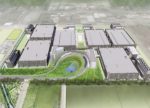
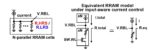
Intel announced that it was going to spend $20B on two new fabs in Arizona and establish Intel Foundry Services as part of re-imagining Intel into “IDM 2.0”. The stated goal would be to provide foundry services to customers much as TSMC does so well today.
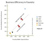
This will not be easy. A lot of companies have died on that hill or been wounded. Global Foundries famously gave up. Samsung still spends oodles of money trying to keep within some sort of distance to TSMC. UMC, SMIC and many others just don’t hold a candle to TSMC’s capabilities and track record.
This all obviously creates a very strange dynamic where Intel is highly dependent upon TSMC’s production for the next several years but then thinks it can not only wean itself off of TSMC’s warm embrace but produce enough for itself as well as other customers to be a real foundry player.
If Pat Gelsinger can pull this off he deserves a billion dollar bonus
This goes beyond doubling down on Intel’s manufacturing and well into a Hail Mary type of play. This may turn out to be an aspirational type of goal in which everyone would be overjoyed if they just caught back up to TSMC.
Like Yogi Berra said “It’s Deja Vu all over again”- Foundry Services 2.0
Lest anyone conveniently forget, Intel tried this Foundry thing before and failed, badly. It just didn’t work. They were not at all competitive.
It could be that we are just past the point of remembering that it was a mistake and have forgotten long enough to try again.
We would admit that Intel’s prior attempt at being a foundry services provider seemed almost half hearted at best. We sometimes thought that many long time Intel insiders previously snickered at being a foundry as they somehow thought it beneath them.
Trying to “ride the wave” of chip shortage fever?
It could also be that Intel is trying to take advantage of the huge media buzz about the current chips shortage by playing into that theme, and claiming to have the solution.
We would remind investors that the current chip shortage that has everyone freaked out will be long over, done and fixed and a distant memory before the first brick is even laid for the two new fabs Intel announced today. But it does make for good timing and PR.
Could Intel be looking for a chunk of “Chips for America” money?
Although Intel said on the call that government funding had nothing to do with whether or not they did the project we are certain that Intel will have its hand out and lobby big time to be the leader of Chips for America.
We would remind investors that the prior management of Intel was lobbying the prior White House administration hard to be put in charge of the “Chips for America” while at the exact same time negotiating to send more product (& jobs) to TSMC.
This is also obviously well timed as is the current shortage. Taken together the idea of Intel providing foundry services makes some sense on the surface at least.
Intel needs to start with a completely clean slate with funding
We think it may be best for Intel to start as if it never tried being a foundry before. Don’t keep any of the prior participants as it didn’t work before.
Randhir Thakur has been tasked with running Intel Foundry Services. We would hope that enough resources are aimed at the foundry undertaking to make it successful. It needs to stand alone and apart.
Intel’s needs different “DNA” in foundry- two different companies in one
The DNA of a Foundry provider is completely different than that of being an IDM. They both do make chips but the similarity stops there.
The customer and customer mindset is completely different. Even the technology is significantly different from the design of the chips, to the process flows in the fabs to package and test. The design tools are different, the manufacturing tools are different and so is packaging and test equipment.
While there is a lot of synergy between being a fab and an IDM it would be best to run this as two different companies under one corporate roof. It’s going to be very difficult to share: Who gets priority? Who’s needs come first? One of the reason’s Intel’s foundry previously failed was the the main Intel seemed to take priority over foundry and customers will not like the obvious conflict which has to be managed.
Maybe Intel should hire a bunch of TSMC people
Much as SMIC hired a bunch of TSMC people when it first started out, maybe Intel would be well served to hire some people from TSMC to get a jump start on how to properly become a real foundry. It would be poetic justice of a US company copying an Asian company that made its bones copying US companies in the chip business.
We have heard rumor that TSMC is offering employees double pay to move from Taiwan to Arizona to start up their new fab there. Perhaps Intel should offer to triple pay TSMC employees to move and jump ship. It would be worth their while. Intel desperately needs the help.
Pat Gelsinger is bringing back a lot of old hands from prior years at Intel as well as others in the industry (including a recent hire from AMAT) but Intel needs people experienced in running a foundry and dealing with foundry customers. Intel has to hire a lot of new and experienced people because they not only need people to catch up their internal capacity, which is not easy, and it needs more people to become a foundry company and the skillsets, like the technology are completely different. This is not going to be either cheap or easy.
I don’t get the IBM “Partnership”
IBM hasn’t been a significant, real player in semiconductors in a very, very long time. It may have a bunch of old patents but it has no significant current process technology that is of true value. It certainly doesn’t build current leading edge or anything close nor does it bring anything to the foundry party.
Its not like IBM helped GloFo a lot. They brought nothing to the table. GloFo still failed in the Moore’s law race. In our view IBM could be a net negative as Intel has to “think different” to be two companies in one, it needs to re-invent itself.
The IBM “partnership” is just more PR “fluff” just like the plug from Microsoft and quotes from tech leaders in the industry that accompanied the press release. Its nonsense.
Don’t go out and buy semi equipment stocks based on Intel’s announcements
Investors need to stop and think how long its going to be before Intel starts ordering equipment for the two $10B fabs announced. Its going to be years and years away.
The buildings have to be designed, then built before equipment can even be ordered. Maybe if we are lucky the first shovel goes in the ground at the end of 2021 and equipment starts to roll in in 2023…maybe beginning production at reasonable scale by 2025 if lucky. Zero impact on current shortage – Even though Intel uses the current shortage as excuse to restart foundry
The announcement has zero, none, nada impact on the current shortage for two significant reasons;
First, as we have just indicated it will be years before these fabs come on line let alone are impactful in terms of capacity. The shortages will be made up for by TSMC, Samsung, SMIC, GloFo and others in the near term. The shortages will be ancient history by the time Intel gets the fabs on line.
Second, as we have previously reported, the vast majority of the shortages are at middle of the road or trailing edge capacity made in 10-20 years old fabs on old 8 inch equipment. You don’t make 25 cent microcontrollers for anti-lock brakes in bleeding edge 7NM $10B fabs, the math doesn’t work. So the excuse of getting into the foundry business because of the current shortage just doesn’t fly, even though management pointed to it on the call.
Could Intel get Apple back?
As we have said before, if we were Tim Apple, a supply chain expert, and the entire being of our company was based on Taiwan and China we might be a little nervous. We also might push our BFF TSMC to build a gigafab in the US to secure capacity. The next best thing might be for someone else like Intel or Samsung to build a gigafab foundry in the US that I could use and go back to two foundry suppliers fighting for my business with diverse locations.
The real reason Intel needs to be a foundry is the demise of X86
Intel has rightly figured out that the X86 architecture is on a downward spiral. Everybody wants their own custom ARM, AI, ML, RISC, Tensor, or what ever silicon chip. No one wants to buy off the rack anymore they all want their own bespoke silicon design to differentiate the Amazons from the Facebooks from the Googles.
Pat has rightly figured out that its all about manufacturing. Just like it always was at Intel and something TSMC never stopped believing. Yes, design does still matter but everybody can design their own chip these days but almost no one, except TSMC, can build them all.
Either Intel will have to start printing money or profits will suffer near term
We have been saying that Intel is going to be in a tight financial squeeze as they were going to have reduced gross margins by increasing outsourcing to TSMC while at the same time re-building their manufacturing, essentially having a period of almost double costs (or at least very elevated costs).
The problem just got even worse as Intel is now stuck with “triple spending”. Spending (or gross margins loss) on TSMC, re-building their own fabs and now a third cost of building additional foundry capacity for outside customers.
We don’t see how Intel avoids a financial hit.
Its not even sure that Intel can spend enough to catch up let alone build foundry capacity even if it has the cash
We would point out that TSMC has the EUV ASML scanner market virtually tied up for itself. They have more EUV scanners than the rest of the world put together.
Intel has been a distant third after Samsung in EUV efforts. If Intel wants to get cranking on 7NM and 5NM and beyond it has a lot of EUV to buy. It can’t multi-pattern its way out of it. Add on top of that a lot of EUV buying to become a foundry player as the PDKs for foundry process rely a lot less on the tricks that Intel can pull on its own in house design and process to avoid EUV. TSMC and foundry flows are a lot more EUV friendly.
As we have previously pointed out the supply of EUV scanners can’t be turned on like a light switch, they are like a 15 year old single malt, it takes a very long time to ramp up capacity, especially lenses which are a critical component.
I don’t know if Intel has done the math or called their friends at ASML to see if enough tools are available. ASML will likely start building now to be ready to handle Intel’s needs a few years from now if Intel is serious.
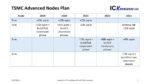
Being a foundry is even harder now
Intel was asked on the call “what’s different this time” in terms of why foundry will work now when it didn’t years ago and their answer was that foundry is a lot different now.
We would certainly agree and suggest that being a leading edge foundry is even much more difficult now. Its far beyond just spending money and understanding technology. Its mindset and process. Its not making mistakes. To underscore both TSMC and Pat Gelsinger its “execution, execution & execution” We couldn’t agree more. Pat certainly “gets it” the question is can he execute?
The tough road just became a lot tougher
Intel had a pretty tough road in front of it to catch the TSMC juggernaut. The road just got a lot more difficult to both catch them and beat them at their own game, that’s twice as hard.
However we think that Pat Gelsinger has the right idea. Intel can’t just go back to being the technology leader it was 10 or 20 years ago, it has to re-invent itself as a foundry because that is what the market wants today (Apple told them so).
It’s not just fixing the technology , it’s fixing the business model as well, to the new market reality.
It’s going to be very, very tough and challenging but we think that Intel is up for it. They have the strategy right and that is a great and important start.
All they have to do is execute….
Related:
Intel Will Again Compete With TSMC by Daniel Nenni
Intel’s IDM 2.0 by Scotten Jones
Intel Takes Another Shot at the Enticing Foundry Market by Terry Daly