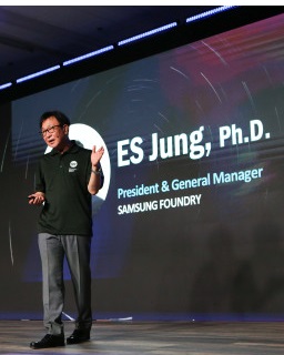
 IEDM is a premier semiconductor conference so it was certainly appropriate for Samsung to do the keynote since they are the largest and one of the most innovative semiconductor companies in the world, absolutely.
Samsung is also one of the more interesting semiconductor companies since they do it all: chip design, semiconductor manufacturing, consumer electronics, and foundry services. Having worked with Samsung many times throughout my career, which included numerous trips to Seoul, I will offer my experience, observation, and opinion, but first let’s talk a bit about the keynote.
Dr. ES Jung, President and GM of the Samsung Foundry business, did the keynote. He started with a joke stating that ES stands for engineering samples which got quite a few laughs, especially from me. ES is a career Samsung employee (he started in 1985) and has spearheaded research and development of advanced logic and memory process technologies and now leads foundry services.
Here is the abstract for his presentation. Remember, IEDM is a conference not a trade show so everyone does papers with abstracts and references:
4th Industrial Revolution and Foundry: Challenges and Opportunities
Abstract—Semiconductor has been the key enabler in the advancement of electronics for the past 50 years. With the coming of 4th industrial revolution, semiconductor will continue to play an even greater role as we invite a wide variety of new applications into our lives, including smart cars, smart factories, artificial intelligence, data centers, robots, etc. Such importance of semiconductor is attributed to its unique ability to copy and create everything human beings imagine. In this paper, the roles of foundry in the 4th industrial revolution, as the entity to turn ideas into reality along with electronic design automation (EDA), intellectual property (IP) vendor, and outsourced semiconductor assembly and test (OSAT) companies, as well as the need for global open innovation to overcome imminent challenges will be discussed.
I also have the slides but I’m not able to share them due to conference guidelines. It is a shame too because there are some very interesting ones. The presentation is in three parts: Industrial Revolution and Semiconductor History, Foundry, Challenges and Opportunities for Innovation.
I’m a big history fan because you really need to know how you got to where you are today to better plan for where you are going tomorrow, right? We have all seen the semiconductor history slides and know semiconductors are a critical part of modern life but it’s nice to be reminded before you get into the really interesting foundry and innovation slides.
With Samsung we have come full circle with the foundry business which started when IDMs had extra fab space that they rented out. Unfortunately, when IDM fabs filled up, the foundry business was shelved, which is what happened to Intel Foundry and is now quietly but officially shut down. The rest is history, pure-play foundries took over and have dominated the fabless chip business for more than 30 years now.
An important part of the foundry business was the ability to multi source to get the best pricing and availability. I remember being involved with a design that was sourced to four different 40nm fabs (TSMC, UMC, SMIC, and Chartered). Some fabless companies were loyal to one fab but that was rare. Now multi sourcing one design to multiple fabs is not possible. In fact, at the leading edge you now only have two foundry choices (TSMC and Samsung). You can certainly use both fabs for different designs and moving forward many companies will do just that, my opinion.
This brings me to the realization I had watching the Samsung keynote. In my dealings with Samsung the most important thing I learned is that they do not give up which is critical in the foundry business. I remember many years ago Samsung told me during one of my visits that they were going to be the number one semiconductor company in the world and here they are. Today, if Samsung told me they were going to be the number one foundry in the world I would not bet against it.
Currently TSMC ($32B+) is the number one foundry by a very large margin with GF ($6B+), UMC (>$5B+), Samsung (>$5B+), and SMIC $3B+) barely visible in the rearview mirror. My prediction today is that Samsung and TSMC will share the majority of the foundry business in the coming years with UMC and GF joining the ranks of the boutique foundries. SMIC is the big question since they have the upper hand in the Chinese market but lack the leading edge innovation. Remember, China buys more chips than the rest of the world and that number will only increase in the years to come, my opinion.
So, my prediction for leading edge wafers in 2025 is that TSMC will have 60% market share and Samsung 40%. I will make my case in the comments section.
Share this post via:


Musk’s Orbital Compute Vision: TERAFAB and the End of the Terrestrial Data Center