Sanjay Jha is taking over as CEO of GlobalFoundries. His background is in mobile. He was at Qualcomm in the early part of his career and was COO from 2006 to 2008 before going to be co-CEO of Motorola and then, when the company was split, CEO of Motorola Mobility. That was acquired by Google and he stepped down after the acquisition closed.… Read More

The Future of Intel
There have been a lot of articles and discussion on SemiWiki about Intel. These articles have all been written from the perspective of an outsider commenting on what Intel is doing, or should or shouldn’t be doing. I thought it would be interesting to take a look at how Intel got to where they currently are, what their current strengths… Read More
Intel Wafer Pricing Exposed!
One of the big questions on Intel’s foundry strategy is: Can they compete on wafer pricing? Fortunately there are now detailed reports that support what most of us fabless folks already know. The simple answer is no, Intel cannot compete with TSMC or Samsung on wafer pricing at 28nm, 20nm, and 14nm.
In fact, recent reports have shown… Read More
Semicon Technology Advancement – A View From IEDM

As I see the semiconductor industry going through significant changes and advances, yet ironically plagued by a growing perception that the pace of scaling is slowing, I was inclined to take a peek into what the industry experts say about the state of the industry and the future of Moore’s Law. Fortunately, at last week’s International… Read More
TSMC: 3D, 450mm, CoWoS and More
The first keynote at the Burlingame 3D conference was by Doug Yu of TSMC. Not surprisingly he was talking about 3D. In particular, TSMC has WLSI technology that they call CoWoS, which stands for chip-on-wafer-on-substrate which pretty much describes how it is built. This is the technology that Xilinx uses for its recently announced… Read More
Should Intel Offer Foundry Services?

This has been a heated topic since Intel announced that it would open its manufacturing facilities to the fabless ecosystem more than a year ago. I for one think it is a colossal mistake and I’m not surprised that many others share this view. IDM’s offering of excess manufacturing capacity to semiconductor design companies… Read More
Could FD-SOI be Cheaper too?
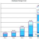
We agree now that FD-SOI technology is Faster, Cooler, Simpler. But can it also be a cheaper technology? Let start with an overview of the current estimation of the development cost for complex SoC on advanced technology nodes. The following data are extracted from International Business Strategies, Inc 2013 report. The first… Read More
The Leading Edge Depends on What You Are Doing
At Semicon Japan a few days ago, Subi Kengeri of GlobalFoundries delivered the keynote. While he covered a number of topics, using Tokyo’s recent win of the 2020 Olympics as a hook, one major theme was the increasing importance of processes other than the bleeding edge digital processes that get all the news.
What is leading… Read More
Intel Comes Clean on 14nm Yield!

Hopefully this blog will result in a meaningful discussion on truth and transparency, and how Intel can do better in regards to both. Take a close look at the manufacturing slides presented by William Holt, Executive Vice President General Manager, Intel Technology and Manufacturing Group. You can see the slide deck HERE. Slide… Read More
Intel’s Tale of Two Cities

It was a year ago that Paul Otellini made his surprise announcement that he was stepping down as CEO of Intel. Soon after, I wrote an article asserting that the only correct choice for his replacement was Nvidia’s CEO Jen Hsun Huang. I went beck to reread what I wroteand I can scarcely say I would change anything I put in the article assuming… Read More
TSMC CoWoS versus Intel EMIB Semiconductor Packaging