In the rapidly evolving landscape of semiconductor manufacturing, the demand for processors that handle increasing workloads while maintaining power efficiency and compact form factors has never been higher. Intel’s Foveros 2.5D packaging technology emerges as a pivotal innovation, enabling denser die integration and enhanced functionality without substantially expanding the physical footprint of chip packages. Introduced in 2019, Foveros 2.5D represents an advanced die-stacking process that assembles multiple chiplets (small specialized silicon dies) into a cohesive unit. This approach addresses the limitations of traditional packaging by layering active dies, such as logic, memory, or FPGAs, atop a passive base die equipped with through-silicon vias (TSVs). The base die, often called a silicon interposer, facilitates seamless interconnectivity, marking a shift from monolithic chip designs to heterogeneous, modular systems.
At the core of Foveros 2.5D is its face-to-face chip-on-chip bonding mechanism, achieved through an ultra-fine microbump pitch of 36 micrometers. This precision bonding minimizes wire parasitics—undesirable electrical properties like resistance, capacitance, and inductance that degrade performance due to interconnect layouts. By reducing these parasitics, Foveros 2.5D ensures higher interconnect density, which is crucial for high-performance applications in data centers, AI accelerators, and edge computing. Furthermore, the technology allows designers to combine advanced process nodes for cutting-edge components with mature nodes for cost-effective, proven IP blocks. This hybrid strategy not only optimizes yields but also lowers manufacturing expenses, as smaller specialized dies on advanced nodes can be paired with reusable elements on established processes.
The benefits of Foveros 2.5D extend beyond density and cost. By stacking components vertically rather than spreading them horizontally, it significantly reduces signal travel distances, thereby lowering latency and boosting overall system performance. This vertical integration also enables more compact designs, ideal for space-constrained devices like mobile processors and embedded systems. When paired with Intel’s Embedded Multi-die Interconnect Bridge (EMIB), Foveros evolves into EMIB 3.5D, expanding reticle limits and supporting even more intricate multi-die configurations. This synergy allows for the connection of passive dies, further enhancing scalability for complex chip architectures.
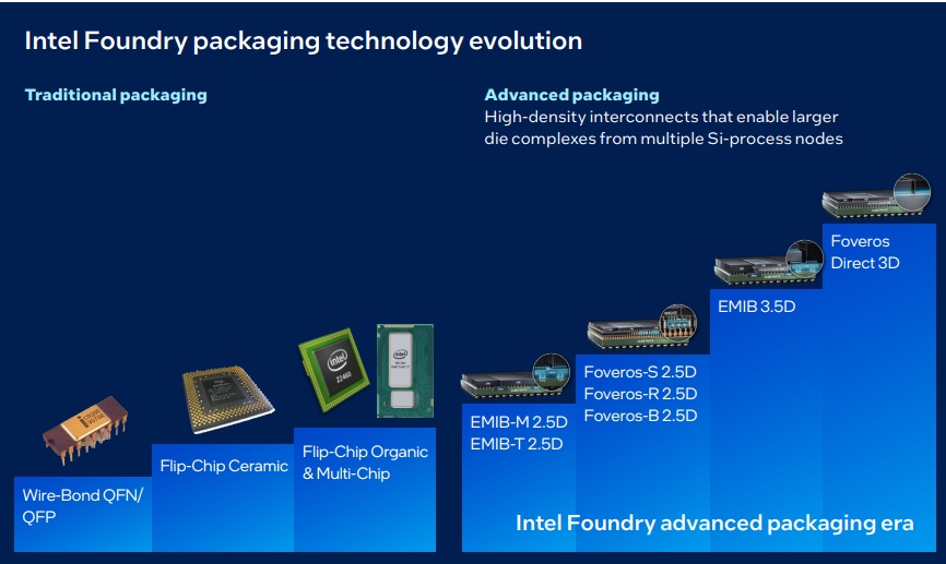
Intel Foundry offers a versatile portfolio of Foveros 2.5D variants to cater to diverse needs. Foveros-S 2.5D employs a silicon interposer to position multiple chips side-by-side, delivering superior performance and power efficiency over conventional methods. In contrast, Foveros-R 2.5D prioritizes cost optimization and interconnect density by eliminating the interposer and utilizing fanout with up to three redistribution layers, enabling flexible heterogeneous systems. For applications requiring multiple base die chiplets, Foveros-B 2.5D integrates active and passive silicon bridges with RDLs, paving the way for future enhancements like cache disaggregation, integrated voltage regulators (IVRs), or metal-insulator-metal capacitors. All these configurations align with the Universal Chiplet Interconnect Express (UCIe) specification, an open industry standard that Intel helped pioneer. UCIe facilitates high-density integration of chiplets from various vendors, promoting interoperability, energy efficiency, and bandwidth gains through asynchronous and synchronous communication.
The evolution of Intel’s packaging technologies—from wire-bond and flip-chip methods to advanced solutions like Foveros—underscores a paradigm shift toward “systems of chips.” This disaggregated approach, championed by Intel Foundry’s Advanced System Assembly & Test, supports full-stack solutions that accelerate time-to-market for demanding use cases. With geographically diverse manufacturing capacity and ecosystem partners for system technology co-optimization, Intel is positioning itself as a leader in the transition from system-on-chip to multi-chiplet ecosystems.
Bottom line: Foveros 2.5D exemplifies how innovative packaging can unlock new frontiers in semiconductor performance, efficiency, and scalability. By enabling heterogeneous chiplet integration, it not only meets current computational demands but also anticipates future challenges in AI and high-performance computing. As Intel continues to drive standards like UCIe, the technology promises to democratize advanced silicon design, fostering collaboration across the industry and ensuring that complex, power-efficient systems become the norm rather than the exception.
Share this post via:


Comments
There are no comments yet.
You must register or log in to view/post comments.