The trend is undeniable. Highly integrated monolithic chips can no longer handle the demands of next-generation systems. The reasons for this significant shift in design are many. Much has been written on the topic; you can get a good overview of the forces at play in multi-die design here. These changes represent the next chapter in the pursuit of exponential scaling originally defined by Moore’s Law. So, it is quite natural to look to Intel, the birthplace of Moore’s Law, for a peek at what lies ahead. Read on to see how Intel enables the multi-die revolution with packaging innovation.
The Packaging Challenge
The move to multi-die systems creates substantial design and manufacturing challenges. Billions of transistors are now spread across multiple dies integrated with complex package form factors containing millions of bump connections. The resultant heterogeneous integration demands a silicon, package and board co-design approach.
Conventional approaches to these challenges often involve a silicon interposer to implement a “2.5D” integration. Drawbacks of this approach include the cost of the extra silicon and increased design complexity and reduced yield. The number and type of dies that can be integrated is also limited with this approach.
Finding a Better Way – EMIB
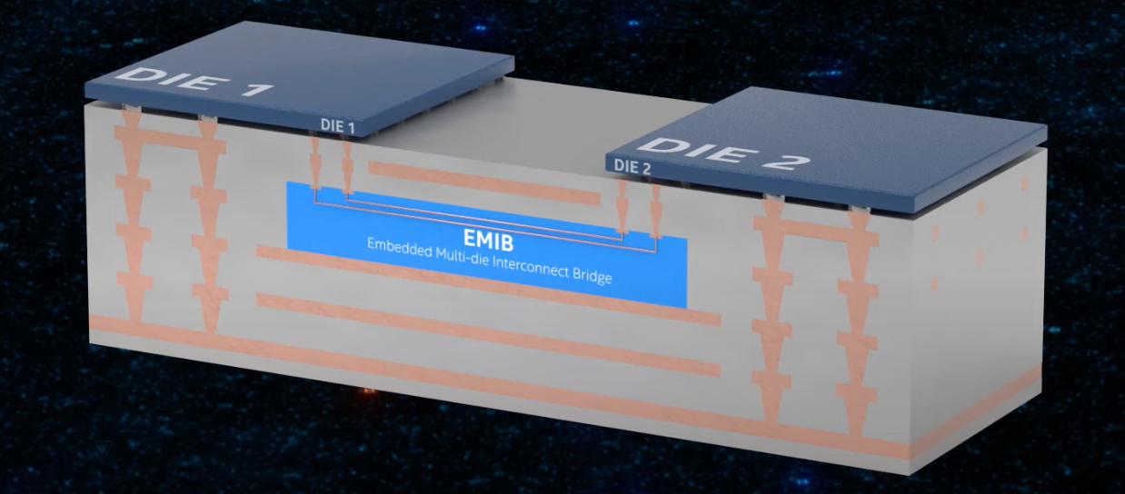
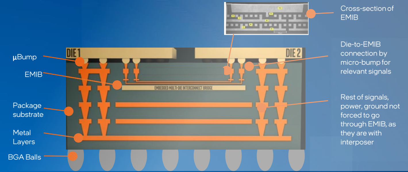
Intel has found a way around many of the current limitations of 2.5D packaging. Embedding a small silicon bridge chip into the package is the answer. EMIB, or embedded multi-die interconnect bridge, delivers a cost-effective way to connect multiple dies within a package. An overview of the approach is provided in the figure below.

A highly scalable capability is delivered with EMIB. There is now flexibility in total design size, number of chiplets bridge dimensions, and localized optimizations to support a wide variety of heterogeneous configurations. EMIB has been proven on several designs, as shown in the figure below.

Implementing EMIB – The Power of the Ecosystem
EMIB-based package design has its own set of challenges. The approach presents high pin count, net count and design density. An example design could contain 24 layers, 52,000 nets and 240,000 pins. All this must be managed across a heterogeneous design flow to achieve low latency and optimal energy efficiency.
Intel Foundry Services (IFS) have repeatedly stated their commitment to bring Intel technology to customers via the industry standard and powerful avenue of a foundry ecosystem. Staying true to that commitment, Intel approached this problem with standards and ecosystem collaboration. Data management, silicon/package/board co-design, consistent modeling/analysis and optimized cost and performance via design reuse are all supported with a comprehensive package assembly design kit (PADK). The PADK contains:
- EMIB Design Guide
- SI/PI Collateral
- Thermal Tolerance
- Mechanical Parameters
- Package Library
- Layout Template
- Padstacks/Pins/Vias
- Parts and Fiducials
- Stack Up
- Thickness
- Tolerance
- Design Rule Specs
- Manufacturing Checks
- Assembly Checks
- Design Rule Checks
- Performance
- Electrical Rules
- Constraints
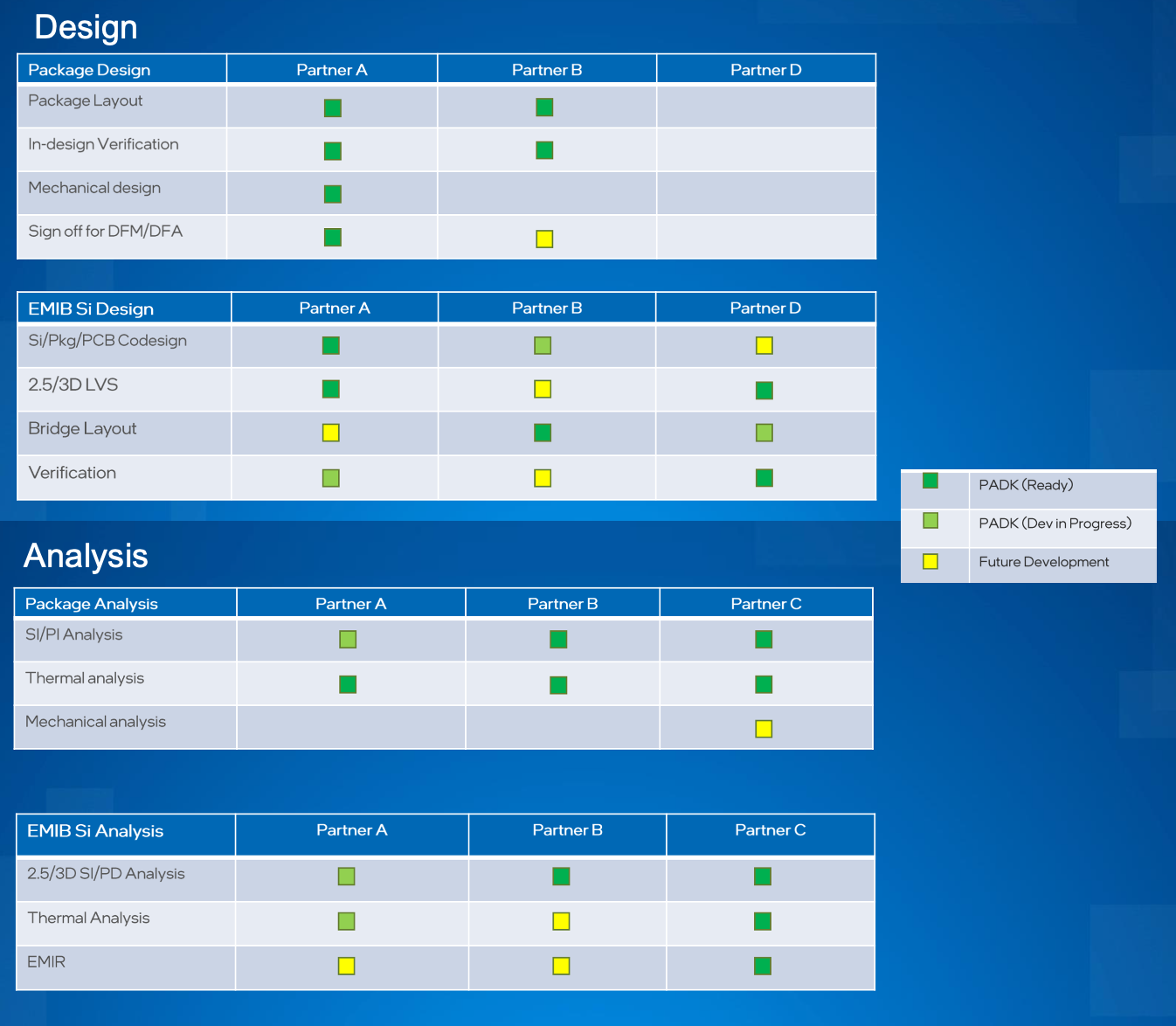
Using this information, Intel built an EMIB-based reference flow with its key EDA partners. There is a design and an analysis reference flow in development. The figure below summarizes the status of each flow across the ecosystem.

What’s Next
There is much more to come from Intel in this area. Additional work includes:
- Die-to-Die IP with UCIe
- Reusability, compatibility, standardization
- EDA-CAD agnostic standards
- Chiplets, tech files, collateral, kits with end-to-end focus for ecosystem development
- EDA framework
- Silicon/package/system co-design
- Interoperable EDA tools, flows and methods
- Data exchange and workflows
The Intel view is that advanced packaging technology, content density, and package complexity requires new methods to drive design efficiency. The focus is to collaborate for ecosystem development using design standards and vendor agnostic tools, flows and methods. And that’s how Intel enables the multi-die revolution with packaging innovation, and IFS delivers it to the external customers.
Also Read:
Intel Internal Foundry Model Webinar
VLSI Symposium – Intel PowerVia Technology
IEDM 2022 – Ann Kelleher of Intel – Plenary Talk
Share this post via:


Comments
2 Replies to “Intel Enables the Multi-Die Revolution with Packaging Innovation”
You must register or log in to view/post comments.