Of the three types of materials used in microelectronics – i.e., semiconductors, metals, and dielectrics – the first two often get the most attention. Yet, there is a pressing need for a rich variety of dielectric materials in device fabrication and interconnect isolation to satisfy the performance, power, and reliability constraints of current microelectronic products. Indeed, advances in dielectrics have been at the heart of the continued scaling achieved in advanced nodes. (High-k gate dielectrics, for example.)
Additionally, the chemical properties of dielectric materials are critical in many process steps, from their use as a patterned hard mask to serve as a protective etch barrier to their use as a sidewall spacer to enable selective epitaxial growth on exposed silicon. Dielectric materials need to support a multitude of deposition techniques, from chemical vapor deposition for isotropic addition on the surface topography to spin-on dielectric coatings to fill trenches.
Research in new dielectric materials is crucial, to support aggressive power, performance, yield, and reliability targets. At the recent IEDM conference, Intel presented two papers describing some of their research (and other contributions) into the introduction of new dielectrics, and an interesting approach toward the corresponding metal interconnect fabrication. [1, 2] This article summarizes the highlights of these presentations.
Background
As briefly mentioned above, dielectrics are required to satisfy a multitude of requirements:
- device gate oxide
Traditional Dennard scaling of the SiO2 gate oxide tox, with dielectric constant k~3.9-4.0, reached a non-manufacturable limit over a decade ago. (For each new process generation, the multiplier for tox is 1/S, where the scaling factor S>1.)
New high-k gate dielectrics were required, to maintain the gate-to-channel electric field, while ensuring a sufficiently thick oxide layer to be manufacturable – i.e., uniformity, low defect density, low leakage current, low trap density, high dielectric breakdown strength. Common examples are SiON, HfO2, HfSiON, and Al2O3.
Devices in each new process are now quoted with an effective gate oxide thickness, using SiO2 as the reference: k(high-k)/tox(high-k) = k(SiO2)/tox_effective. For example, if the target scaled tox_effective ~3nm, a 16nm HfO2 gate oxide layer would be fabricated, helping to achieve the manufacturability goals listed above.
- M-I-M capacitors
High-k dielectrics are also crucial to the fabrication of metal-insulator-metal (decoupling) capacitors in the back-end-of-line fabrication, as illustrated below. [3]

The goal is to provide a high capacitance per um**2 , with minimal impact to available global routing tracks.
- interlayer dielectrics (ILDs) surrounding interconnects
In this case, low-k dielectric materials have been introduced to reduce the parasitic capacitance (and thus, the R*C time constant) of interconnects. Prior to the mid-90s, deposited SiO2 was the prevalent ILD, subsequently replaced with alternative low-k oxides – e.g., carbon-doped oxides, such as SiCOH (aka, “Black Diamond”, a TM of Applied Materials). [4]
Ongoing R&D into these ILD materials has drive the dielectric constant to k~2.3, a marked improvement over SiO2. Recently, air gap dielectrics (k=1, ideal) have been introduced into BEOL processing – more on air gaps shortly.
A concern is the structural integrity of these ILD materials, due to their greater porosity. This is especially true for low-k ILDs at higher metal levels, due to the stress introduced by the thermal expansion differences between the silicon die, encapsulation material, and package – delamination issues of the BEOL metal layers is a known failure mechanism.
There are also (very thin layer) dielectrics needed in the metal stack to serve as copper diffusion barriers. (The diffusivity of CU into high-porosity ILDs is high.)
- etch stops/etch barriers
A hard mask dielectric is patterned on top of a material which is to be protected during a process etch step. The HM needs to have a very low etch rate relative to the exposed material being removed. In a subsequent etch step, the HM needs to have a very high etch rate to the surrounding materials (assuming the HM is not a “leave-behind” layer).
- dielectric deposition
To date, the majority of dielectric deposition process steps provide an isotropic layer over the die surface topography, whether using a chemical vapor deposition or spin-on method.
In a self-aligned, double-patterning process, a subsequent anisotropic etch step is used to provide “sidewall spacers”, as illustrated in the figure below. [3]
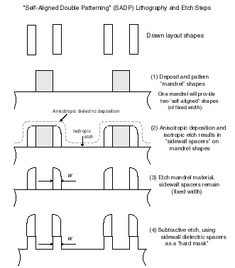
These spacers offer a unique, controlled method for several key process steps: definition of fins for FinFET devices; adding a dielectric between gate and source/drain nodes (with the spacer serving as a HM for subsequent S/D epitaxial growth).
Recent research is focused on a novel selective deposition process, where dielectric materials are deposited on specific die surfaces only – more on this unique method shortly.
New ILDs
Intel reported results on alternative ILDs to the current SiCOH-based low-k materials, using boron carbides (BCH) and boron nitrides (BNH). The figure below illustrates the dielectric constant versus Young’s Modulus for various ILD materials. (Young’s Modulus, or the “Modulus of Elasticity”, is an indication of the deformity of a material when subjected to stress forces – a higher coefficient implies less deformation.)
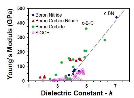
Note that while the dielectric constant for SiCOH is indeed low, the material strength is poor – alternatives with comparable k and higher strength are attractive.
ILDs for Subtractive Etch Metals
There is also active research into alternative interconnect metals to Cu, specifically Ruthenium. The prevalent method for fabricating Cu wires and vias uses the formation of dual damascene trenches, with initial barrier/seed layers prior to Cu deposition. This is followed by chemical-mechanical polishing (CMP) for surface planarization.
The potential introduction of Ru as an interconnect metal has renewed interest in patterning using subtractive etch – a deposited metal layer is masked, then etched, as was the case for Aluminum wires used prior to the transition to Cu. In this case, deposition of the ILD is done after metal patterning – a flowable dielectric is an attractive option for filling the (high-aspect ratio) volume between the wires.
Selective Dielectric Deposition
For advanced process nodes, as illustrated above, a self-aligned, dual patterning (SADP) step is pursued to enable an aggressive pitch of etched layers, as an alternative to the cost of multipatterning lithography/etch process sequences. Clearly, a lot of process steps are required to implement SADP.
An attractive alternative would be to implement selective deposition of the dielectric material (e.g., as an etch barrier). The Intel IEDM paper shared research results on a “bottom-up” area-selective atomic layer deposition approach.
The figure on the left below illustrates selective deposition processes of interest: dielectric deposition on an exposed metal surface (capping layer), dielectric deposition for trench fill, and selective sidewall dielectric deposition. The figure on the right shows dielectric deposition on an existing dielectric but not the adjacent metal.

The figure on the right illustrates an approach to selective deposition — the wafer is pre-treated with a material which preferentially forms self-assembled monolayers on a specific surface. Subsequently, atomic layer deposition of the dielectric does not nucleate and grow on this pre-treated area.
One specific application of selective deposition is illustrated below.
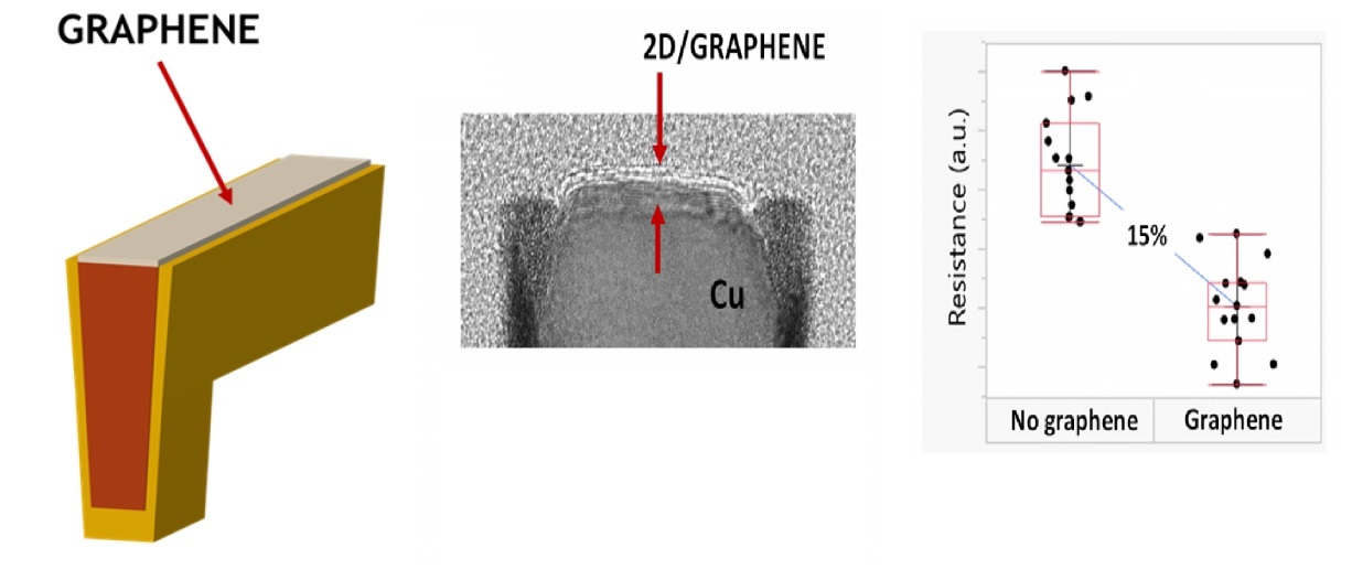
The use of graphene as an (atomically-thin) capping layer for Cu interconnects has been shown to improve (reduce) Cu line resistivity, compared to current capping dielectrics. (A 15% experimental reduction in Cu resistivity is shown — that’s a major improvement.)
There are challenges, to be sure – the deposition selectivity should be high and the defect density low. Nevertheless, selective dielectric deposition holds great promise to reduce fabrication process complexity.
Air Gap Dielectrics
The optimum ILD dielectric constant is 1, associated with an air gap between interconnects. Intel has previously described their process for fabrication of air gaps, as illustrated below. [5] After (damascene) metal patterning, the dielectric between the metal lines is etched, a thin diffusion barrier is added, and the next layer ILD is deposited and planarized.
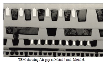
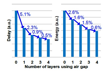
An example of the delay/energy benefits of air gap dielectrics is shown below – the (simulated) circuit example is a datapath multiplier.
Dual Metal Layer Thickness
At IEDM, Intel also presented results from R&D efforts to provide two metal line thicknesses for an interconnect layer.
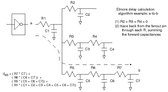
This option allows unique selection of line R and C values that comprise the R*C time constant, for optimal “tuning” of wire delays. A first-order Elmore delay model for an RC interconnect tree is illustrated below, with the resulting effective point-to-point R*C summation equation. [3] Note the strong dependence of the delay on the initial wire R values. A dual-metal thickness option would offer unique R and C combinations along the fanout paths.
The process flow for fabrication of metal thicknesses a-only, b-only, a+b, and vias is depicted graphically and with TEMs in the figures below. (The option for fabricating air gaps between the two metal thicknesses is also shown.)


Layer ‘a’ and the vias utilize a dual-damascene process flow, while layer ‘b’ is single-damascene, followed by CMP. Note the depth and aspect ratio of the air gap is quite high, to minimize the coupling capacitance values between adjacent wires, regardless of their thickness.
The figures below illustrate calculated values and testsite measurements for Cwire and R*C time constant for various interconnect thickness configurations: all b; all a+b; b alternating with a+b; a+b alternating with b; with and without air gap dielectrics.
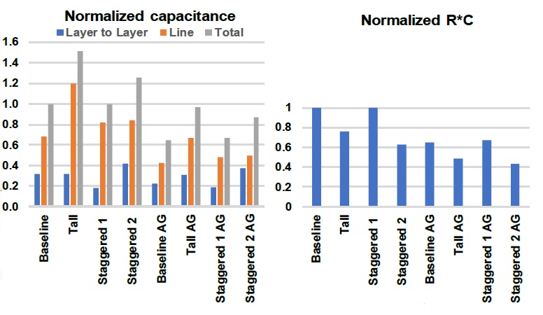
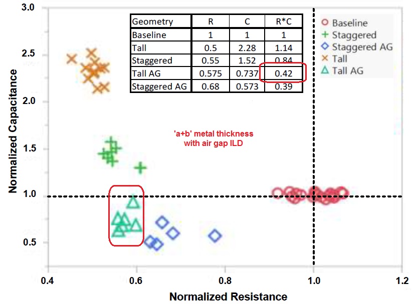
(Note that there is still the requirement to model the wire thickness tolerances due to CMP removal variation due to local interconnect density ranges.)
An example from Intel where separate R and C optimizations might be useful is shown below.
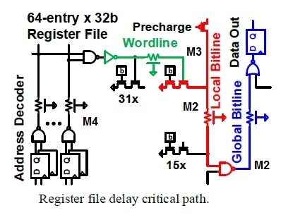
For a register file, the R*C delay product is more impactful for the address decode and word-line drivers (in M4 and M3), whereas C optimization may be the focus for (local and global M2) bitline implementations.
Summary
The demands on dielectric materials are great, from low-k ILDs to high-k gate oxides. Hard mask etch stops require differentiated etch chemistry to surrounding layers. New selective dielectric deposition methods offer the potential for significant process cost savings.
Although perhaps less captivating than new semiconductor and metallization materials being pursued, investigations into improved dielectrics is crucial to the PPA, yield, and reliability roadmap for microelectronics. At IEDM, Intel provided an update on the activity that they and other researchers are pursuing. I would encourage you to review their presentations.
-chipguy
References
[1] King, S., et al, “A Selectively Colorful yet Chilly Perspective on the Highs and Lows of Dielectric Materials for CMOS Nanoelectronics”, IEDM 2020, Paper 40.1
[2] Lin, Kevin, et al, “Staggered Metallization with Air gaps for Independently Tuned Interconnect Resistance and Capacitance”, IEDM 2020, paper 32.5.
[3] Dillinger, T., VLSI Design Methodology Development, Prentice-Hall, 2019.
[4] https://svmi.com/service/low-k-films/
[5] Fischer, K., et al, “Low-k interconnect stack with multi-layer air gap and tri-metal-insulator-metal capacitors for 14nm high volume manufacturing”, IEEE Intl. Interconnect Technology Conference, May, 2015.
[6] Hashemi, F., et al, “Selective Deposition of Dielectrics: Limits and Advantages of Alkanethiol Blocking Agents on Metal-Dielectric Patterns”, ACS Applied Materials and Interfaces, Nov 2016.
Share this post via:


Comments
There are no comments yet.
You must register or log in to view/post comments.