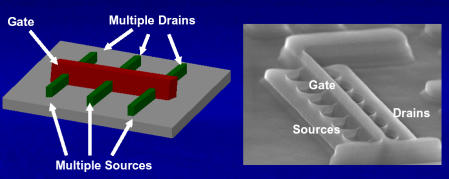
 Thanks to SemiWiki readers for the feedback and comments on the previous “Introduction to FinFET Technology” posts – very much appreciated! The next installment on FinFET modeling will be uploaded soon.
In the interim, Dan forwarded the following link to me “ Intel’s FinFETs too complicated and difficult, says Asenov“, which provides some (preliminary) analysis on FinFET behavior, from recently published TEM pictures of Intel’s Ivy Bridge designs:
There is both important and (somewhat) misleading information in this article – yet, it serves as a good basis for the upcoming discussion on FinFET modeling.
The key takeaway from this article is that the contour and width of the fin is a strong factor on the resulting device behavior.
The gate input voltage results in an electric field through the gate dielectric. This field terminates on free carriers in the body of the fin, if the magnitude of the gate-to-source input exceeds the Vt of the device. When a voltage difference is present between drain and source terminals, the free carrier concentration and mobility define the device current.
The contours of the fin where the curvature is largest will have the densest electric field, and thus the highest carrier density, in both the “on” (Vgs > Vt) and “subthreshold leakage” (Vgs <= Vt) conditions. (There is also a “quantum effect” that modulates the available density of free carrier states in the fin which we'll ignore, for now.)
For narrow fins, there is another benefit to transistor performance. The carrier mobility is less at the “surface channel” due to increased scattering. Carriers that terminate the gate electric field in the body of the fin away from the surface will have greater mobility when a drain-source potential is applied. The thickness of the carrier “inversion layer” in the fin is also a critical parameter to device current.
These FinFET characteristics are (somewhat) evident in the figures in the article.
However, I would take issue with some of the other conclusions being drawn.
“Intel’s FinFET’s too complex and difficult” – that’s a bold statement, when Ivy Bridge processors are in volume production. Intel’s device R&D and process development teams have optimized the FinFET profile for manufacturability, but “too complex and difficult” is not substantiated.
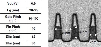
“SOI FinFET’s would be easier…” That’s also a very bold statement. The dielectric below the thin silicon layer in an SOI wafer does provide a more natural etch stop for the fin height. Yet, the theme of the article is engineering the (final) fin contour, which is common fabrication challenge for both SOI and bulk. Specifically, there are variations in contour and dimension for SOI fins, as well – see the TEM photograph from a recent IBM paper at the VLSI Symposium 2012.

(SOI FinFET 22nm process node; the dark areas are the fins, with a “hard mask” dielectric on top — a “dual-gate” configuration; from Lin, et al, “Channel Doping Impact on FinFET’s for 22nm”, VLSI Symposium 2012.)
From the analysis provided, the variation in fin dimensions from a (small) sample of TEM photos on Ivy Bridge parts results in a small variation in on-current, which appears to contradict the title of the article. Further, the analysis does not include consideration of other key sources of variation in fabrication – just the fin contour.
So, the net is: FinFET’s are extremely complex to fabricate and model. The contour and width of the fin is an important, but certainly not the only consideration, for analysis of (statistical variations in) device current. Intel has made some key fabrication decisions at 22nm for Ivy Bridge parts to enhance manufacturability – to state that “Intel’s FinFET’s are too complex and difficult” is not justified.
Just my $0.02… Look for a FinFET modeling post soon.
Reference:
Introduction to FinFET Technology Part I
Introduction to FinFET Technology Part II
-chipguy
Share this post via:


Comments
One Reply to “Intel’s finfets too complex and difficult?”
You must register or log in to view/post comments.