GLOBALFOUNDRIES (GF) recently announced they were abandoning 7nm and focusing on “differentiated” foundry offerings in a move our own Dan Nenni described as a “pivot”, a description GF appears to have embraced. Last week GF held their annual Technology Conference and we got to hear more about the pivot from new CEO Tom Caulfield including why GF abandoned 7nm and what their new focus is.
GLOBALFOUNDRIES Pivoting away from Bleeding Edge Technologies
Background
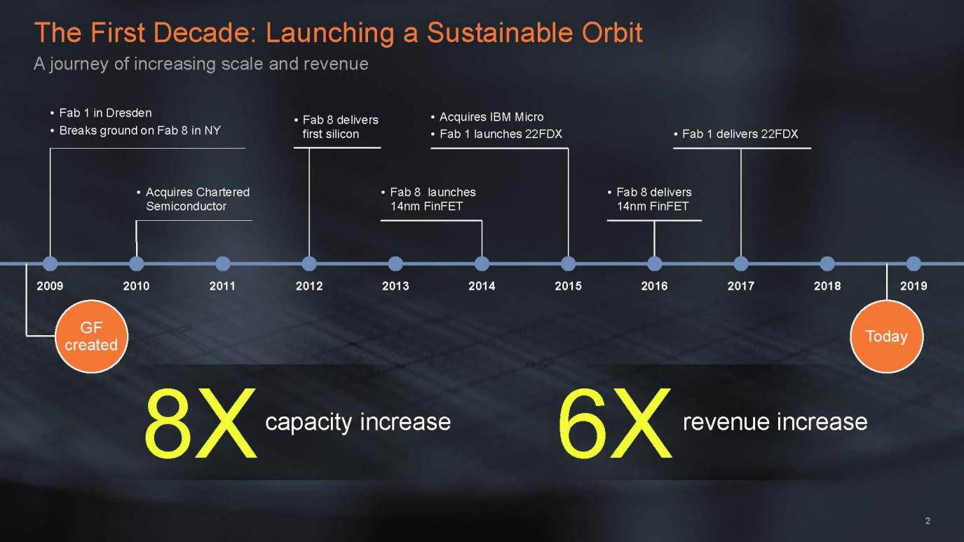
GF was created in 2008 in a spin-out of the fabs formerly owned by AMD. In 2010 GF acquired Chartered Semiconductor, the number three foundry in the world at that time and in 2015 GF acquired IBM’s microelectronics business. Figure 1 illustrates the key milestones in GF’s history.

Figure 1. GLOBALFOUNDRY Milestones
GF is owned by Mubadala Development Company (MDC). MDC financials include the technology segment made up of GF. Based on Mubadala financial disclosures, from 2016 to 2017 GF grew revenues by 12.4% and saw their operating loss widen from 8.0% of revenue in 2016 to 27.2% of revenue in 2017 calling into question the sustainability of GF’s business model.
On March 9[SUP]th[/SUP], 2018 Tom Caulfield became the new CEO of GF with a mandate to build a sustainable business model.
7nm History
In the early 2010s GF was working on development of their own 14nm process technology but realizing they were falling behind their competitors ultimately abandoned their in-house development and licensed 14nm from Samsung. The licensed 14nm process was launched in 2014 in Fab 8 (see figure 1). GF has continued to improve on that process adding process options and more recently launching a shrunk 12nm version. The 14nm and newer 12nm version have been utilized by AMD for microprocessors and graphics processors, by GF for their FX-14 ASIC platform and by other customers.
With the IBM Microelectronics acquisition in 2015, GF received a significant infusion of researchers including Gary Patton who became the CTO of GF. Beginning around 2016, the combined GF and IBM research teams started to develop their own in-house 7nm technology. The initial version was planned to be based on optical exposures with GF also planning an EUV based follow-on version.
By all account’s development was proceeding well. In a July 2017 SemiWiki exclusive, GF disclosed their key 7nm process density metrics and at IEDM in December 2017 GF disclosed additional process details. My write up of GF’s process density metrics is available here and a comparison of GF’s 7nm process to Intel’s 10nm from IEDM is available here. GF’s 7nm process appeared to be a competitive process. I have also written about the leading-edge 7nm and beyond processes here.
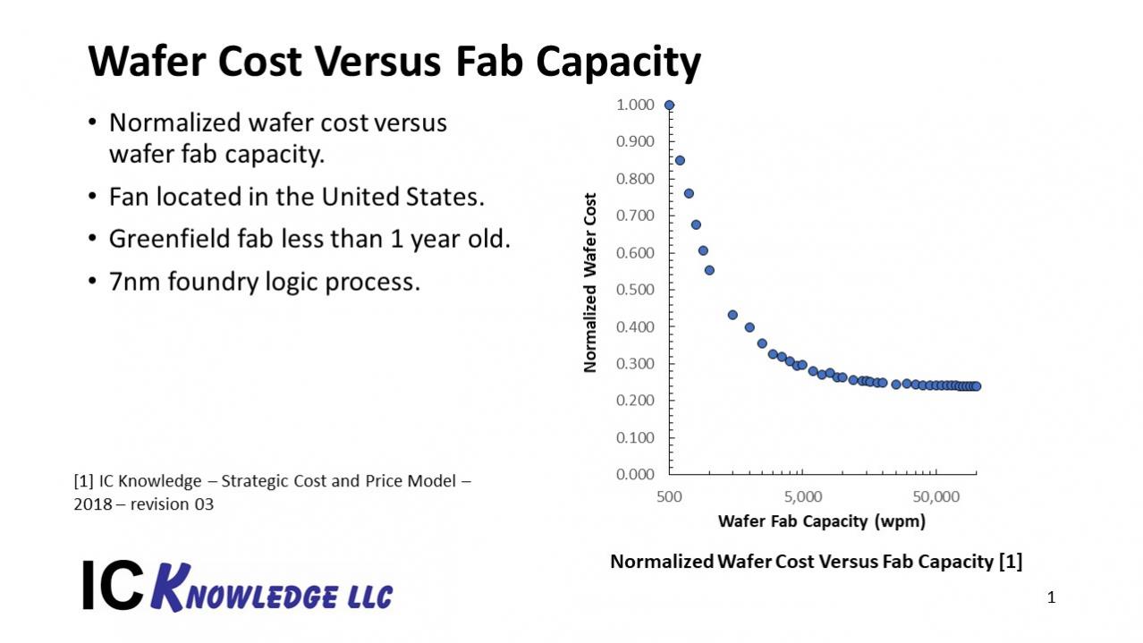
One concern I have had about GF 7nm for a long time is scale. GF was reportedly installing only 15,000 wafers per month (wpm) of 7nm capacity. The average 300mm foundry fab had 34,213 wpm capacity at the end of 2017 and are projected to reach over 40,343 wpm by the end of 2020, and 43,584 wpm by the end of 2025 [1]. Newer leading-edge fabs are even larger and are what is driving up the average. At the leading-edge, wafer cost is roughly 60% depreciation and larger fabs have better equipment capacity matching and therefore higher capital efficiency and lower costs. Figure 2 illustrates the wafer cost versus fab capacity for a wafer fab in the United States running a 7nm process calculated using the IC Knowledge – Strategic Cost and Price Model – 2018 – revision 03 for a greenfield fab.

Figure 2. Wafer Cost Versus Fab Capacity for 7nm Fab in the United States
Even though 15,000 wpm is past the steepest part of the curve there is still several hundred dollars in cost per wafer advantage for larger capacity wafer fabs.
Tom Caulfield also mentioned GF needed $3 billion dollars of additional capital to get to 12,000 wpm and they could only fund half of it through cash flow, they would have to borrow the other half and the projected return wasn’t good.
Customer Inputs
When Tom took over as CEO he went out on the road and visited GF’s customers. What he found was a lack of commitment to GF’s 7nm process in the customer base. Many customers were never going to go to 7nm and of the customers who were, GF wouldn’t have enough capacity to meet their demands. There was also concern in the customer base that 7nm would take up all the R&D and capital budgets and starve the other processes they wanted to use of investment.
What Did GF Give Up?
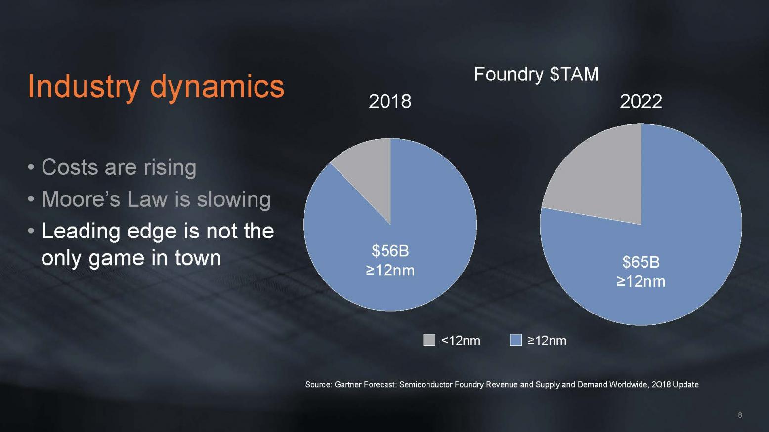
By exiting the 7nm and smaller wafer market GF has given up some opportunity. Figure 3 illustrates the total available market (TAM) for foundry wafers in 2018 and 2022. Even in 2022 the forecast is for 7nm to be less than 25% of the market and the TAM for >=12nm to increase from $56 billion dollars in 2018 to $65 billion dollars in 2022.

Figure 3. Foundry Market
In terms of specific markets, GF are conceding some of the computing, graphic processing and data center opportunity. Currently AMD is GF’s largest customer and long term that business will presumably shrink as AMD moves to smaller geometries.
What Now?
GF will be focused on four major “differentiated – feature rich” offerings going forward.
[LIST=1]
Conclusion
GFs’s pivot away from 7nm has aligned the companies R&D and capital spending more closely with their customers needs. Whether GF can build a sustainable business model on the four business segments they are now focused on remains to be seen but more closely aligning your companies focus with your customers’ needs certainly appears to be a step in the right direction.
[1] IC Knowledge – 300mm Watch Database – 2018 – revision 02
Share this post via:


Musk’s Orbital Compute Vision: TERAFAB and the End of the Terrestrial Data Center