“Mobile is the largest platform ever built by humanity”, Christiano Amon, Executive Vice President, Qualcomm Technologies, Inc. and President, Qualcomm CDMA Technologies speaking at the GLOBALFOUNDRIES Technologies Conference (GTC) 2017.
RF is poised for enormous growth in applications beyond mobile phones. Assisted driving is becoming prevalent in automotive with multiple radars for lane departure, collision warning, blind spot detection and parking assistance. As vehicles transition from assisted driving to self-driving, enormous volumes of data will have to be uploaded into the cloud on a real-time basis. The whole emerging Internet Of Things (IOT) space is made up of smart sensors that transmit data up to the cloud for health monitoring, smart buildings, industrial applications and more.
Cristiano further stated that over $12 trillion dollar in 5G related goods and services are expected in 2035 as the unifying fabric for mobile, automotive and IOT.
“Everything now has a radio”, Bami Bastani, Senior Vice President of the RF Business Unit at GLOBALFOUNDRIES (GF) speaking at the GTC.
RF has unique requirements that drive specialized technologies and GF is uniquely positioned to service these requirements with the industry’s broadest RF offering.
RF Requirements
RF applications can be characterized based on the operating frequency and the required power level. Current 4G Cell phone handsets operate over several bands around 850, 900, 1,800 and 1,900 MHz with power requirements of around a half a watt. As cellular service transitions to 5G the initial implementation is expected to be sub 6GHz solutions in the range of 3 to 5 GHz. Longer term 5G may migrate into the millimeter Wave regime of 30 to 300 GHz for higher throughput. Cellular base stations operate at the same frequencies as the handsets but require power in the 100-watt range. IOT may operate over a wider range of frequencies but at much lower power of around 10 milliwatts. Automotive radar will also be low power due to the relatively short-range requirements (uo to 200 to 300 meters) but will operate at higher frequencies with 24GHz and 77GHz being preferred bands. Figure 1 summarizes the frequency and power requirements of selected RF applications.
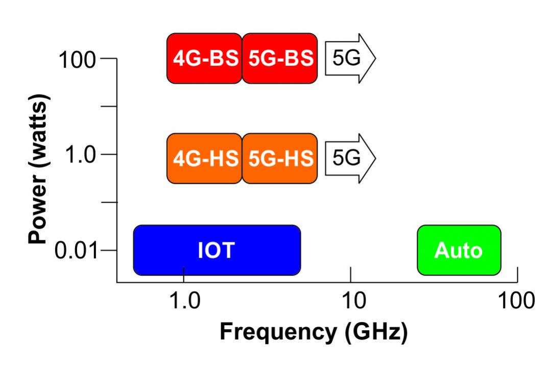
Figure 1.Frequency and power requirements of selected RF applications.
In figure 1. HS = hand set, BS = base station and Auto = automotive radar.
RF Systems
Each RF system has its own set of functional blocks to achieve a design goal. Mobile phones have become increasingly complex to support voice and data over a variety of bands. The front end of mobile phones have multiple antennas with complex switching, filtering and tuning requirements. Figure 2 illustrates some of the key functional blocks in the RF section of a cell phone.

Figure 2.Cell phone main RF signal path.
In figure 2 the Application Processor is the brains of the cell phone and is a complex multiple core System-On-A-Chip (SOC) fabricated in the latest/densest logic process node. Currently state-of-the-art applications processors are ramping up in 10nm processes and 7nm applications processors are expected next year. Table 1 compares the logic density in Mgates/mm2 for selected GF process options.
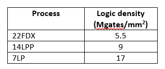
Table 1.Logic gate density for selected GF processes.
As you can see from table 1, for complex logic chips the leading-edge logic processes provide the highest density and therefore the smallest chip.
The transceiver is typically a less complex logic design and is dominated by analog and RF circuits. Typically the transceiver is produced in a process that is one or two nodes behind the application processor. Today a 14FF or 28nm process would be typical for the cellular transceiver.
The green area in figure 2 are the analog RF functions and they are performed by a variety of specialty RF processes that will be described below. The function inside the green area are:
- LNA – Low Noise Amplifier – amplifies the received signals.
- PA – Power amplifier – amplifies the signals to be transmitted.
- Duplex/filter – filters and selects the frequency bands.
- Mode/band switch – switches between frequency bands.
- TX/RX switch – switched between transmit and receive and the various antennas.
- Antenna tune – tunes the antennas for efficient operation.
- Antennas – multiple antennas are required to support different bands.
Not shown in this simplified figure are the GPS and WiFi RF sections that would also be part of a higher end feature or smart phone.
RF SOI
IBM was the world leader in the production of RF SOI devices prior to the GF acquisition and GF has continued to build on that legacy with over 32 billion RF SOI devices shipped to-date.
RF SOI is based on a partially depleted silicon-on-insulator (PDSOI) process. The starting SOI substrate is very expensive relative to a standard bulk silicon substrate making this a relatively expensive process. PDSOI wafers have relatively thick device silicon layers and relatively thick buries oxide layers.
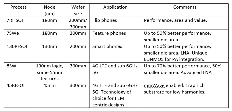
Table 2. GF RF SOI options.
RF SOI key characteristics:
- The technology of choice for RF switching.
- Can make good low noise amplifiers (LNA).
- Can be used for power amplifiers (PA) if the power requirement is in the milliwatts.
SiGe
Silicon Germanium processes are BiCMOS processes that provide the best RF linearity and power handling making them the silicon technology of choice for RF power amplifiers (PA). GF has shipped over 5 billion SiGe PA devices. SiGe competes with gallium arsenide for power amplifier applications providing higher integration with the ability to integrate logic functions.
SiGe BiCMOS processes such as GF manufacturers begin as a base CMOS logic process and then add high performance SiGe bipolar transistors and other RF enhancements. SiGe processes are difficult to shrink and are manufactured at relatively larger nodes limiting the ability to integrate complex logic.
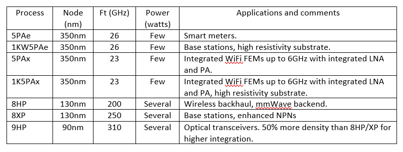
Table 3. GF SiGe process options.
All of GF SiGe processes are manufactured on 200mm wafers.
SiGe key characteristics:
- The silicon technology of choice for power amplifiers (PA). The PA processes are good for a few watts and the HP processes for several watts.
- The technology of choice for stand-alone high performance low noise amplifiers (LNA).
- Not good for switching.
- Low density logic relative to smaller nodes. 9HP has a density of 0.4 million gates/mm[SUP]2[/SUP] versus 5.5, 9 and 17 for 22FDX, 14LPP and 7LP respectively (table 1).
RF CMOS
RF CMOS is a standard bulk CMOS process with added modules such as RF optimized interconnect, metal-insulator-metal (MIM) capacitors, precision resistors and thick metal inductors. RF CMOS is relatively inexpensive compared to RF SOI but also offers generally lower performance.
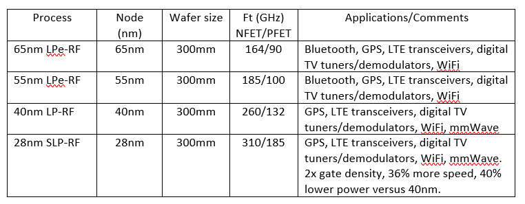
Table 4. GF RF CMOS process options.
RF CMOS key characteristics:
- Low cost.
- Good logic density at smaller nodes,
- Can make good low noise amplifiers (LNA).
- Can be used for power amplifiers (PA) if the power requirement is in the milliwatts.
FDX
The FDX platform is a Fully Depleted SOI (FDSOI) technology. The thin silicon device layers and thin buried oxide layers enable back biasing to be used to tune the device performance and power consumption. FDX combines relatively dense CMOS logic with excellent analog and RF performance at the lowest available power. FDX is the technology of choice where a high degree of integration with superior RF, analog and mmWave performance is a key goal.
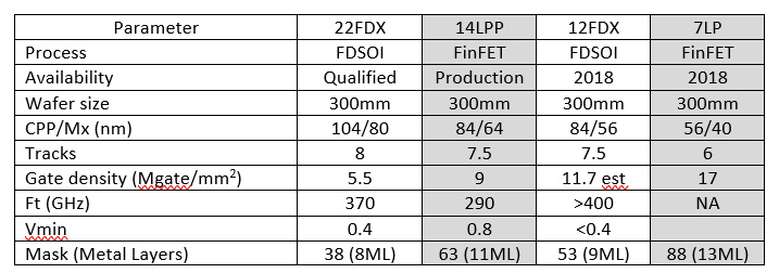
Table 5. GF FDSOI (FDX) process options. FinFET processes shown in grey for comparison.
FDSOI key characteristics:
- Lower cost than comparable FinFET process with similar logic performance.
- Good logic density enabling fully integrated designs if the logic requirements aren’t too high.
- Lowest operating voltage and power.
- Excellent RF with lower current and higher Gm for comparable speed to FinFETs.
- Excellent analog performance.
Discussion
RF is a large and growing application space within the semiconductor market. Assisted/autonomous driving, mobile and IOT should continue to drive rapid RF growth for the next decade and beyond. Emerging RF applications like 5G and assisted/autonomous driving will require higher frequencies into the mmWave range. IOT applications will require highly integrated and inexpensive solutions with the lowest possible power consumption.
Smart phone applications processors are large/complex CMOS logic SOCs that require the densest CMOS logic possible. GF’s 14LPP and forthcoming 7LP are positioned to address this space. Baseband/transceiver chips can be address by trailing edge 40nm and 28nm processes and eventually by 14LPP.
For antenna switching RF SOI is the solution of choice. For low RF power applications, the LNA and even PA may also be integrated. For higher power applications or where the highest performance is required SiGe is the technology of choice for PA and LNA applications.
For low cost and less demanding applications such as GPS, Bluetooth and older WiFi RF CMOS is the best option.
The emerging FDX platform is ideal for IOT applications where an analog interface is needed to connect to a sensor, digital logic is required for processing and then RF is required for wireless data transmission. On 22FDX, Front End module functionality typically implemented in RF SOI can now be integrated with the transceiver, baseband processor and PMIC for a true single chip SoC, optimized for cost sensitive applications like IOT. FDX can combine these requirement at the lowest possible power consumption to enable years of operation from a single battery. The FDX platform may also find applications providing greater mobile phone front end integration.
Conclusion
GF has the broadest portfolio of RF silicon solutions in the industry. With leading edge CMOS, RF CMOS, SiGe, RF SOI and FDSOI process technologies all available at multiple nodes GF can provide complete RF solutions.


Chemical Origins of Environmental Modifications to MOR Lithographic Chemistry