There have been a multitude of announcements recently relative to the incorporation of machine learning (ML) methods into EDA tool algorithms, mostly in the physical implementation flows. For example, deterministic ML-based decision algorithms applied to cell placement and signal interconnect routing promise to expedite and optimize physical design results, without the iterative cell-swap placement and rip-up-and-reroute algorithms. These quality-of-results and runtime improvements are noteworthy, to be sure.
Yet, there is one facet of the semiconductor industry that is (or soon will be) critically-dependent upon AI support – the metrology of semiconductor process characterization, both during initial process development/bring-up, and in-line inspection driving continuous process improvement. (Webster’s defines metrology as “the application of measuring instruments and testing procedures to provide accurate and reliable measurements”.) Every aspect of semiconductor processing, from lithographic design rule specifications to ongoing yield analysis, is fundamentally dependent upon accurate and reliable data for critical dimension (CD) lithographic patterning and material composition.
At the recent VLSI 2020 Symposium, Yi-hung Lin, Manager of the Advanced Metrology Engineering Group at TSMC, gave a compelling presentation on the current status of semiconductor metrology techniques, and the opportunities for AI methods to provide the necessary breakthroughs to support future process node development. This article briefly summarizes the highlights of his talk. [1]
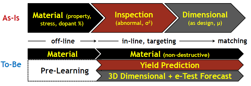
The figure below introduced Yi-hung’s talk, illustrating the sequence where metrology techniques are used. There is an initial analysis of fabrication materials specifications and lithography targets during development. Once the process transitions to manufacturing, in-line (non-destructive) inspection is implemented to ensure that variations are within the process window for high yield. Over time, the breadth of different designs, and specifically, the introduction of the process on multiple fab lines requires focus on dimensional matching, wafer-to-wafer, lot-to-lot, and fab line-to-fab line.

The “pre-learning” opportunities suggest that initial process bring-up metrology data could be used as the training set for AI model development, subsequently applied in production. Ideally, the models would be used to accelerate the time to reach high-volume manufacturing. These AI opportunities are described in more detail below.
Optical Critical Dimension (OCD) Spectroscopy
I know some members of the SemiWiki audience fondly (or, perhaps not so fondly) recall the many hours spent in the clean room looking through a Zeiss microscope at wafers, to evaluate developed photoresist layers, layer-to-layer alignment verniers, and material etch results. At the wavelength of the microscope light source, these multiple-micrometer features were visually distinguishable – those days are long, long gone.
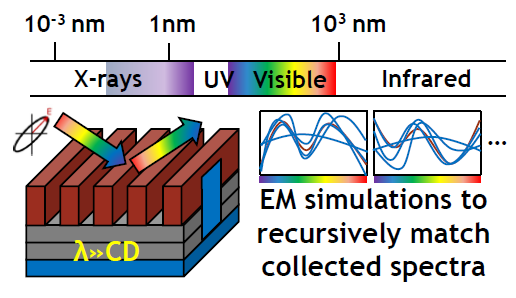
Yi-hung highlighted that OCD spectroscopy is still a key source of process metrology data. It is fast, inexpensive, and non-destructive – yet, the utilization of OCD has changed in deep sub-micron nodes. The figure below illustrates the application of optical light sources in surface metrology.

The incident (visible, or increasingly, X-ray) wavelength is provided to a 3D simulation model of the surface, which solves electromagnetic equations to predict the scattering. These predicted results are compared to the measured spectrum, and the model is adjusted – a metrology “solution” is achieved when the measured and EM simulation results converge.
OCD illumination is most applicable when an appropriate (1D or 2D) “optical grating-like” pattern is used for reflective diffraction of the incident light. However, the challenge is that current surface topographies are definitely three-dimensional, and the material measures of interest do not resemble a planar grating. Optical X-ray scatterometry provides improved analysis accuracy with these 3D topographies, but is an extremely slow method of data gathering.
Yi-hung used the term ML-OCD, to describe how an AI model derived from other metrology techniques could provide an effective alternative to the converged EM simulation approach. As illustrated below, the ML-OCD spectral data would serve as the input training dataset for model development, with the output target being the measures from (destructive) transmission electron microscopy (TEM), to be discussed next.

ML for Transmission Electron Microscopy (TEM)
TEM utilizes a focused electron beam that is directed through a very thin sample – e.g., 100nm or thinner. The resulting (black-and-white) image provides high-magnification detail of the material cross-section, due to the much smaller electron wavelength (1000X smaller than an optical photon).

There are two areas that Yu-hing highlighted where ML techniques would be ideal for TEM images. The first would utilize familiar image processing and classification techniques to automatically extract CD features, especially useful for “blurred” TEM images. The second would be to serve as the training set output for ML-OCD, as mentioned above. Yi-hung noted that one issue to the use of TEM data for ML-OCD modeling is that a large amount of TEM sample data would required as the model output target. (The fine resolution of the TEM image compared to the field of the incident OCD exposure exacerbates the issue.)
ML for Scanning Electron Microscopy (SEM)
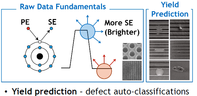
The familiar SEM images measure the intensity of secondary electrons (emitted from the outer atomic electron shell) that are produced from collisions with an incident primary electron – the greater the number of SE’s generated in a local area, the brighter the SEM image. SEMs are utilized at deep submicron nodes for (top view) line/space images, and in particular, showing areas where lithographic and material pattering process defects are present.

ML methods could be applied to SEM images for defect identification and classification, and to assist with root cause determination by correlating the defects to specific process steps.
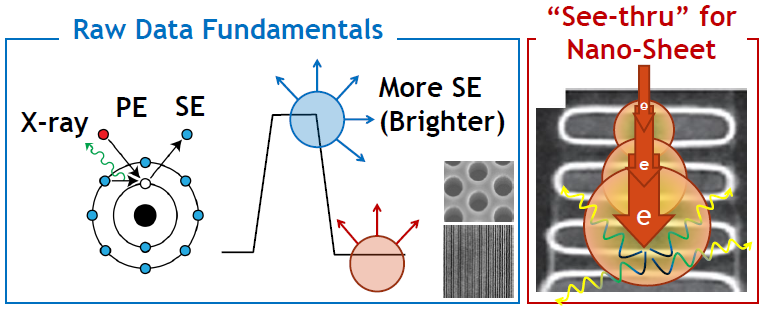
Another scanning electron technique uses a variable range of higher-energy primary electrons, which will have different landing distances from the surface, and thus, provide secondary electrons from deeper into the material. However, an extremely large primary energy will result in the generation of both secondary electrons and X-ray photons, as illustrated below. (Yi-hung noted that this will limit the image usability for the electron detectors used in SEM equipment, and thus limit the material depth that could be explored – either more SE sensitivity or SE plus X-ray detector resolution will be required.) The opportunities for a (generative) machine learning network to assist with “deep SEM” image classification are great.

Summary
Yi-hung concluded his presentation with the following breakdown of metrology requirements:
- (high-throughput) dimensional measurement:
-
- OCD, X-ray spectroscopy (poor on 3D topography)
-
- (high-accuracy, destructive) reference measurement: TEM
- Inspection (defect identification and yield prediction): SEM
- In-line monitoring (high-throughput, non-destructive):
-
- hybrid of OCD + X-ray, with ML-OCD in the future?
-
In all these cases, there are great opportunities to apply machine learning methods to the fundamental metrology requirements of advanced process development and high-volume manufacturing. Yi-hung repeated the cautionary tone that semiconductor engineering metrology currently does not have the volume of training data associated with other ML applications. Nevertheless, he encouraged data science engineers potentially interested in these applications to contact him. 🙂
Yu-hing also added that there is a whole other metrology field to explore for potential AI applications – namely, application of the sensor data captured by individual pieces of semiconductor processing equipment, as it relates to overall manufacturing yield and throughput. A mighty challenge, indeed.
-chipguy
References
[1] Yi-hung Lin, “Metrology with Angstrom Accuracy Required by Logic IC Manufacturing – Challenges From R&D to High Volume Manufacturing and Solutions in the AI Era”, VLSI 2020 Symposium, Workshop WS2.3.
Images supplied by the VLSI Symposium on Technology & Circuits 2020.
Share this post via:


Comments
There are no comments yet.
You must register or log in to view/post comments.