You are currently viewing SemiWiki as a guest which gives you limited access to the site. To view blog comments and experience other SemiWiki features you must be a registered member. Registration is fast, simple, and absolutely free so please,
join our community today!
Dr. Meghali Chopra is co-founder and CEO of SandBox Semiconductor. She is responsible for SandBox’s vision and strategy and oversees the development of SandBox’s software products and technologies. Dr. Chopra received her PhD in Chemical Engineering from the University of Texas at Austin where her research focused … Read More
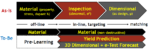
From initial process technology development (TD) to high volume manufacturing (HVM) status for a new node, one of the key support functions to improve and maintain yield is the in-line wafer inspection technology. Actually, there are multiple inspection technologies commonly employed, with tradeoffs in pixel resolution,… Read More
There have been a multitude of announcements recently relative to the incorporation of machine learning (ML) methods into EDA tool algorithms, mostly in the physical implementation flows. For example, deterministic ML-based decision algorithms applied to cell placement and signal interconnect routing promise to expedite… Read More
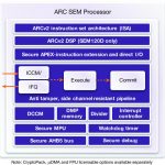
Building devices for the IoT has become especially challenging thanks to two conflicting requirements. The device has to be small and ultra-low power in most applications but also in many of those applications it has to provide a high-level of security, especially to defend high-value targets like smart metering, payment terminals,… Read More
With every new technology node, there are newer physical effects that need to be taken into account. And every new physical effect brings with itself several new formats to model them. Often a format is also associated with several of its derivatives, sometimes an standard reincarnation of a proprietary format further evolved… Read More
MEMS design and fabrication is highly complex in the sense that the fabrication process heavily depends on the design, unlike IC fabrication which has a standard set of processes. A slight change in MEMS design can alter its fabrication steps to a large extent. For example, setting device parameters such as capacitance or linear… Read More
Engineers are always looking to improve the efficiency of how they work, but don’t want to sacrifice accuracy in the process. This is true in the world of semiconductor process development, where traditional build-and-test cycles are both time and resource intensive. But what if there was a way to do certain steps in a ‘virtual’… Read More
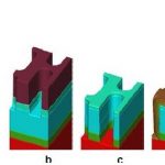
Remember? During DAC2013 I talked about a new kind of innovation: A Virtual Fabrication Platform, SEMulator3D, developed by COVENTOR. Now, to my pleasant surprise, there is something to report on the proven results from this platform. IBM, in association with COVENTOR, has successfully implemented a 3D Virtual Fabrication… Read More