As transistor dimensions shrink to follow Moore’s Law, the functionality of the gate used to switch on or off the current is actually being degraded by the short channel effect (SCE) [1-5]. Moreover, the simultaneous reduction of voltage aggravates the degradation, as will be discussed below.
A Practical Lower Limit of Threshold Voltage
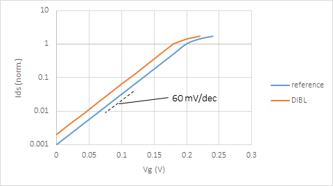
First, we will estimate a practical lower limit for the threshold voltage Vth, i.e., the gate voltage at which the transistor is said to turn on. Below the threshold voltage, the current drops off exponentially, in the best case, at a rate of 60 mV/decade, i.e., every 0.06 V reduction below Vth results in the current dropping to 10% of its value (Figure 1). So we can see that if the leakage current at 0V is to be 0.1% (already a large allowance) of its value at Vth, the threshold voltage must be at least 0.18 V. In turn, the power supply voltage Vdd is expected to be several times Vth, e.g., ~ 1V. 60 mV/decade also means the current changes by a factor of 2 for every 0.02V shift. This is important for considering changes in the threshold voltage itself.
Figure 1. Subthreshold slope of 60 mV/decade gives ~0.1% leakage at 0V for Vth ~0.2V. A 20 mV drain-induced barrier lowering (DIBL) leads to ~2X change in current due to the shift of the Ids vs. Vg curve.
The Short Channel Effect: Drain-Induced Barrier Lowering
Normally, in order to turn the transistor on or off, the gate voltage controls the depletion of charges under the gate, between the source and drain terminals. Basically, as shown in Figure 2, as the gate length Lg is reduced, the source and drain terminals are closer, and the respective depletion layer widths Ws and Wd take up the significant portion of Lg. Specifically, the depths of the source and drain depletion layers cause electric field bending under the gate, which becomes more severe as the source-drain distance is narrowed.
Figure 2. The origin of drain-induced barrier lowering (DIBL). A larger gate (left) has a flat potential contour over most of the gate length, while a shorter gate (right) shows bending of the potential contour.
As a result, when the voltage from the source to drain is increased, the barrier in between is reduced fairly significantly, to the same degree as the voltage on the gate itself. This phenomenon is also known as drain-induced barrier lowering (DIBL). DIBL is generally given as the shift in threshold voltage (the reduction of the barrier) for a given shift in drain-source voltage. Usually the reference drain-source voltage is near zero, while the shifted voltage is near the supply voltage, and the threshold voltage shift is on the order of tens of millivolts. But given that a 20 mV shift already constitutes a factor of 2 change, when Vth ~ 0.2V and Vdd ~ 0.7-1V, a DIBL of 20 mV/V as shown in Figure 1 can therefore be considered an upper limit of tolerance.
Have we already reached minimum Lg?
A minimum gate length of ~20 nm has already been predicted by scientists at IBM [1,5] as well as IMEC [6]. This holds for both SiO2 (minimum 1 nm) and high-k (HfO2 ~4-5 nm) gate dielectrics. It is derived from the characteristic decay length of the lateral electric field under the gate [1].
Figure 3. 2017 field FinFET data showing DIBL degradation for Lg of 20 nm and below [5].
A lower Lg limit of ~20 nm for the planar MOSFET means alternative transistor architectures need to be considered for achieving smaller gate lengths. The most well-known are the FinFET [5] and the surround-gate [7]. On the other hand, a similar Lg limit also appears to have been confirmed by field FinFET data [5] (Figure 3). This is not hard to imagine, as field bending toward the substrate is still possible within the fins. Moreover, in the case of the gate surrounding all sides of the silicon, the gate + 2x oxide thickness (>10 nm) must be added to the silicon body thickness, which hinders scaling of cell height (perpendicular to the gate pitch). By also considering drive current requirements [8], it is also preferred to widen the cell height [7], i.e., there is potential reverse scaling perpendicular to the gate pitch.
Implications
The limitation of the lateral scaling of transistors could portend greater reliance on 3D extension by wafer bonding, such as that implemented in the HBM interface [9]. Or it could be that the future of computing will shift more to memory, particularly those with 3D capacity expansion capability. Thus, the current ongoing developments toward in-memory computing, e.g., [10], are very timely.
References
[1] Y. Taur and T. Ning, Fundamentals of Modern VLSI Devices, 2nd Edition, Cambridge University Press, 2009.
[2] http://www.cs.ucl.ac.uk/staff/ucacdxq/projects/vlsi/report.pdf
[3] https://web.stanford.edu/class/ee316/MOSFET_Handout5.pdf
[4] http://www-inst.eecs.berkeley.edu/~ee130/sp03/lecture/lecture27.pdf
[5] A. Razavieh et al., “Scaling Challenges of FinFET Architecture below 40nm Contacted Gate Pitch,” 75th Annual Device Research Conference, 2017.
[6] http://www1.semi.org/eu/sites/semi.org/files/events/presentations/07_Hans%20Mertens_imec.pdf
[7] N. Loubert et al., “Stacked Nanosheet Gate-All-Around Transistor to Enable Scaling Beyond FinFET,” 2017 Symp. VLSI Technology.
[8] U. K. Das et al., “Limitations on Lateral Nanowire Scaling Beyond 7-nm Node,” IEEE Elec. Dev. Lett. 38, 9 (2017).
[9] https://en.wikipedia.org/wiki/High_Bandwidth_Memory
Share this post via:


Silicon Insurance: Why eFPGA is Cheaper Than a Respin — and Why It Matters in the Intel 18A Era